参数资料
| 型号: | AD674BJN |
| 厂商: | Analog Devices Inc |
| 文件页数: | 12/12页 |
| 文件大小: | 0K |
| 描述: | IC ADC 12BIT MONO 3OUT 28-DIP |
| 产品变化通告: | Product Discontinuance 27/Oct/2011 |
| 标准包装: | 13 |
| 位数: | 12 |
| 采样率(每秒): | 66k |
| 数据接口: | 并联 |
| 转换器数目: | 1 |
| 功率耗散(最大): | 375mW |
| 电压电源: | 双 ± |
| 工作温度: | 0°C ~ 70°C |
| 安装类型: | 通孔 |
| 封装/外壳: | 28-DIP(0.600",15.24mm) |
| 供应商设备封装: | 28-PDIP |
| 包装: | 管件 |
| 输入数目和类型: | 2 个单端,单极;2 个单端,双极 |
REV. C
–9–
TO
OUTPUT
BUFFERS
CE
CS
R/
C
A0
12/
8
NYBBLE A
ENABLE
NYBBLE B
ENABLE
NYBBLE C
ENABLE
NYBBLE = 0
ENABLE
STATUS
CLK EN
HIGH IF CONVERSION
IN PROGRESS
SAR
RESET
EOC 12
EOC 8
START CONVERT
S
R
Q
QB
READ
VALUE OF A0 AT LAST CONVERT COMMAND
D
EN
D
EN
Q
R
S
Q
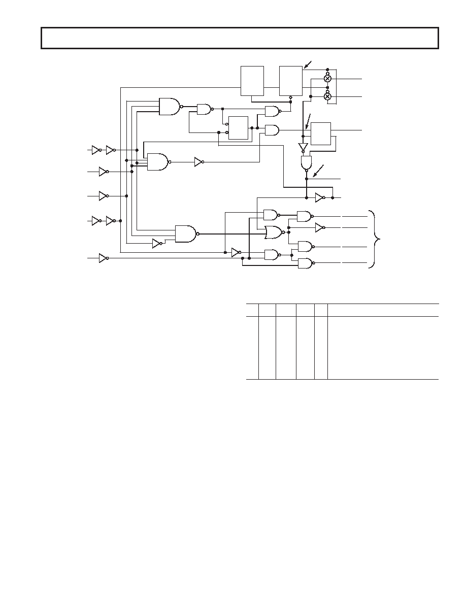
Figure 9. Equivalent Internal Logic Circuitry
CONTROL LOGIC
The AD674B and AD774B contain on-chip logic to provide
conversion initiation and data read operations from signals
commonly available in microprocessor systems; this internal
logic circuitry is shown in Figure 9.
The control signals CE,
CS, and R/C control the operation of
the converter. The state of R/
C when CE and CS are both
asserted determines whether a data read (R/
C = 1) or a convert
(R/
C = 0) is in progress. The register control inputs, A
0 and
12/
8, control conversion length and data format. If a conversion
is started with A0 low, a full 12-bit conversion cycle is initiated.
If A0 is high during a convert start, a shorter 8-bit conversion
cycle results. During data read operations, A0 determines
whether the three-state buffers containing the 8 MSBs of the
conversion result (A0 = 0) or the 4 LSBs (A0 = 1) are enabled.
The 12/
8 pin determines whether the output data is to be orga-
nized as two 8-bit words (12/
8 tied to DIGITAL COMMON)
or a single 12-bit word (12/
8 tied to V
LOGIC). In the 8-bit mode,
the byte addressed when A0 is high contains the 4 LSBs from
the conversion followed by four trailing zeroes. This organiza-
tion allows the data lines to be overlapped for direct interface to
8-bit buses without the need for external three-state buffers.
An output signal, STS, indicates the status of the converter.
STS goes high at the beginning of a conversion and returns low
when the conversion cycle is complete.
Table I. Truth Table
CE
CS R/C 12/8 A
0
Operation
0
XXXX
None
X
1
XXX
None
1
0
X
0
Initiate 12-Bit Conversion
1
0
X
1
Initiate 8-Bit Conversion
1
011X
Enable 12-Bit Parallel Output
1
0100
Enable 8 Most Significant Bits
1
0101
Enable 4 LSBs + 4 Trailing Zeroes
The ADC may be operated in one of two modes, the full-control
mode and the standalone mode. The full-control mode uses all
the control signals and is useful in systems that address decode
multiple devices on a single data bus. The standalone mode is
useful in systems with dedicated input ports available. In gen-
eral, the standalone mode is capable of issuing start-convert
commands on a more precise basis and therefore produces
higher accuracy results. The following sections describe these
two modes in more detail.
FULL-CONTROL MODE
Chip Enable (CE), Chip Select (
CS), and Read/Convert (R/C)
are used to control Convert or Read modes of operation. Either
CE or
CS may be used to initiate a conversion. The state of R/C
when CE and
CS are both asserted determines whether a data
Read (R/
C = 1) or a Convert (R/C = 0) is in progress. R/C
should be LOW before both CE and
CS are asserted; if R/C is
HIGH, a Read operation will momentarily occur, possibly
resulting in system bus contention.
AD674B/AD774B
相关PDF资料 |
PDF描述 |
|---|---|
| AD676BD | IC ADC 16BIT SAMPLING 28-CDIP |
| AD677BD | IC ADC 16BIT SAMPLING 16-CDIP |
| AD678BJ | IC ADC 12BIT SAMPLING 44-JLCC |
| AD679BJ | IC ADC 14BIT SAMPLING 44-JLCC |
| AD7111BQ | IC DAC LOGARITHMIC 16-CDIP |
相关代理商/技术参数 |
参数描述 |
|---|---|
| AD674BJNZ | 功能描述:IC ADC 12BIT MONO 3OUT 28DIP RoHS:是 类别:集成电路 (IC) >> 数据采集 - 模数转换器 系列:- 其它有关文件:TSA1204 View All Specifications 标准包装:1 系列:- 位数:12 采样率(每秒):20M 数据接口:并联 转换器数目:2 功率耗散(最大):155mW 电压电源:模拟和数字 工作温度:-40°C ~ 85°C 安装类型:表面贴装 封装/外壳:48-TQFP 供应商设备封装:48-TQFP(7x7) 包装:Digi-Reel® 输入数目和类型:4 个单端,单极;2 个差分,单极 产品目录页面:1156 (CN2011-ZH PDF) 其它名称:497-5435-6 |
| AD674BJR | 制造商:AD 制造商全称:Analog Devices 功能描述:Complete 12-Bit A/D Converters |
| AD674BKN | 功能描述:IC ADC 12BIT MONO 3OUT 28-DIP RoHS:否 类别:集成电路 (IC) >> 数据采集 - 模数转换器 系列:- 标准包装:1 系列:- 位数:14 采样率(每秒):83k 数据接口:串行,并联 转换器数目:1 功率耗散(最大):95mW 电压电源:双 ± 工作温度:0°C ~ 70°C 安装类型:通孔 封装/外壳:28-DIP(0.600",15.24mm) 供应商设备封装:28-PDIP 包装:管件 输入数目和类型:1 个单端,双极 |
| AD674BKNZ | 功能描述:IC ADC 12BIT MONO 3OUT 28DIP RoHS:是 类别:集成电路 (IC) >> 数据采集 - 模数转换器 系列:- 其它有关文件:TSA1204 View All Specifications 标准包装:1 系列:- 位数:12 采样率(每秒):20M 数据接口:并联 转换器数目:2 功率耗散(最大):155mW 电压电源:模拟和数字 工作温度:-40°C ~ 85°C 安装类型:表面贴装 封装/外壳:48-TQFP 供应商设备封装:48-TQFP(7x7) 包装:Digi-Reel® 输入数目和类型:4 个单端,单极;2 个差分,单极 产品目录页面:1156 (CN2011-ZH PDF) 其它名称:497-5435-6 |
| AD674BKR | 制造商:AD 制造商全称:Analog Devices 功能描述:Complete 12-Bit A/D Converters |
发布紧急采购,3分钟左右您将得到回复。