- 您现在的位置:买卖IC网 > PDF目录10048 > AD678JNZ (Analog Devices Inc)IC ADC 12BIT SAMPLING 28-DIP PDF资料下载
参数资料
| 型号: | AD678JNZ |
| 厂商: | Analog Devices Inc |
| 文件页数: | 4/14页 |
| 文件大小: | 0K |
| 描述: | IC ADC 12BIT SAMPLING 28-DIP |
| 标准包装: | 1 |
| 位数: | 12 |
| 采样率(每秒): | 200k |
| 数据接口: | 并联 |
| 转换器数目: | 2 |
| 功率耗散(最大): | 745mW |
| 电压电源: | 模拟和数字,双 ± |
| 工作温度: | 0°C ~ 70°C |
| 安装类型: | 通孔 |
| 封装/外壳: | 28-DIP(0.600",15.24mm) |
| 供应商设备封装: | 28-PDIP |
| 包装: | 管件 |
| 输入数目和类型: | 1 个单端,单极;1 个单端,双极 |
AD678
REV. C
–12–
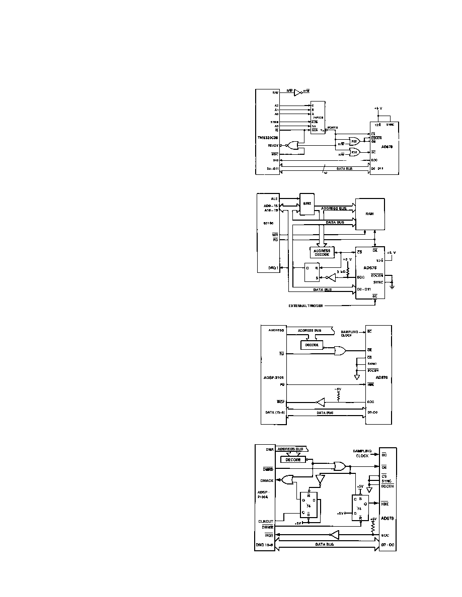
AD678 TO TMS320C25
In Figure 14 the AD678 is mapped into the TMS320C25 I/O
space. AD678 conversions are initiated by issuing an OUT
instruction to Port 8. EOC status and the conversion result are
read in with an IN instruction to Port 8. A single wait state is
inserted by generating the processor READY input from
IS,
Port 8 and
MSC. This configuration supports processor clock
speeds of 20 MHz and is capable of supporting processor clock
speeds of 40 MHz if a NOP instruction follows each AD678
read instruction.
AD678 TO 80186
Figure 15 shows the AD678 interfaced to the 80186 micro-
processor. This interface allows the 80186’s built-in DMA con-
troller to transfer the AD678 output into a RAM based FIFO
buffer of any length, with no microprocessor intervention.
In this application the AD678 is configured in the asynchronous
mode, which allows conversions to be initiated by an external
trigger source independent of the microprocessor clock. After
each conversion, the AD678 EOC signal generates a DMA
request to Channel 1 (DRQ1). The subsequent DMA READ
operation resets the interrupt latch. The system designer must
assign a sufficient priority to the DMA channel to ensure that
the DMA request will be serviced before the completion of the
next conversion. This configuration can be used with 6 MHz
and 8 MHz 80186 processors.
AD678 TO ANALOG DEVICES ADSP-2101
Figure 16 demonstrates the AD678 interfaced to an ADSP-2101.
With a clock frequency of 12.5 MHz, and instruction execution in
one 80 ns cycle, the digital signal processor supports the AD678
interface with one wait state.
The converter is configured to run asynchronously using a sam-
pling clock. The EOC output of the AD678 gets asserted at the
end of each conversion and causes an interrupt. Upon interrupt,
the ADSP-2101 immediately asserts its FO pin LOW. In the
following cycle, the processor starts a data memory read by pro-
viding an address on the DMA bus. The decoded address gener-
ates
OE for the converter, and the high byte of the conversion
result is read over the data bus. The read operation is extended
with one wait state and thus started and completed within two
processor cycles (160 ns). Next, the ADSP-2101 asserts its FO
pin HIGH. This allows the processor to start reading the lower
byte of data. This read operation executes in a similar manner to
the first and is completed during the next 160 ns.
AD678 TO ANALOG DEVICES ADSP-2100A
Figure 17 demonstrates the AD678 interfaced to an ADSP-2100A.
With a clock frequency of 12.5 MHz, and instruction execution
in one 80 ns cycle, the digital signal processor will support the
AD678 data memory interface with three hardware wait states.
The converter is configured to run asynchronously using a sam-
pling clock. The EOC output of the AD678 gets asserted at the
end of each conversion and causes an interrupt. Upon interrupt,
the ADSP-2100A immediately executes a data memory write
instruction which asserts
HBE. In the following cycle, the pro-
cessor starts a data memory read (high byte read) by providing
an address on the DMA bus. The decoded address generates
OE for the converter. OE, together with logic and latch, is used
to force the ADSP-2100A into a one cycle wait state by generat-
ing DMACK. The read operation is thus started and completed
within two processor cycles (160 ns).
HBE is released during
“high byte read.” This allows the processor to read the lower
byte of data as soon as “high byte read” is complete. The low
byte read operation executes in a similar manner to the first and
is completed during the next 160 ns.
Figure 14. AD678 to TMS320C25 Interface
Figure 15. AD678 to 80186 DMA Interface
Figure 16. AD678 to ADSP-2101 Interface
Figure 17. AD678 to ADSP-2100A Interface
相关PDF资料 |
PDF描述 |
|---|---|
| IDT72805LB15PF8 | IC FIFO SYNC DUAL 256X18 128TQFP |
| LT1134AISW | IC 4DRV/4RCV RS232 5V 24-SOIC |
| IDT72V241L15PFI | IC FIFO SYNC 4KX9 15NS 32QFP |
| AD9222ABCPZRL7-50 | IC ADC 12BIT SRL 50MSPS 64LFCSP |
| IDT72V241L10PFG | IC FIFO SYNC 4KX9 10NS 32QFP |
相关代理商/技术参数 |
参数描述 |
|---|---|
| AD678JP | 制造商:未知厂家 制造商全称:未知厂家 功能描述:Analog-to-Digital Converter, 12-Bit |
| AD678KD | 功能描述:IC ADC 12BIT SAMPLING 28-CDIP RoHS:否 类别:集成电路 (IC) >> 数据采集 - 模数转换器 系列:- 产品培训模块:Lead (SnPb) Finish for COTS Obsolescence Mitigation Program 标准包装:250 系列:- 位数:12 采样率(每秒):1.8M 数据接口:并联 转换器数目:1 功率耗散(最大):1.82W 电压电源:模拟和数字 工作温度:-40°C ~ 85°C 安装类型:表面贴装 封装/外壳:48-LQFP 供应商设备封装:48-LQFP(7x7) 包装:管件 输入数目和类型:2 个单端,单极 |
| AD678KN | 制造商:Analog Devices 功能描述:ADC Single Flash 200ksps 12-bit Parallel 28-Pin PDIP W |
| AD678KNZ | 功能描述:IC ADC 12BIT SAMPLING 28DIP RoHS:是 类别:集成电路 (IC) >> 数据采集 - 模数转换器 系列:- 标准包装:1 系列:- 位数:14 采样率(每秒):83k 数据接口:串行,并联 转换器数目:1 功率耗散(最大):95mW 电压电源:双 ± 工作温度:0°C ~ 70°C 安装类型:通孔 封装/外壳:28-DIP(0.600",15.24mm) 供应商设备封装:28-PDIP 包装:管件 输入数目和类型:1 个单端,双极 |
| AD678KP | 制造商:未知厂家 制造商全称:未知厂家 功能描述:Analog-to-Digital Converter, 12-Bit |
发布紧急采购,3分钟左右您将得到回复。