参数资料
| 型号: | AD679BJ |
| 厂商: | Analog Devices Inc |
| 文件页数: | 4/16页 |
| 文件大小: | 0K |
| 描述: | IC ADC 14BIT SAMPLING 44-JLCC |
| 标准包装: | 1 |
| 位数: | 14 |
| 采样率(每秒): | 128k |
| 数据接口: | 并联 |
| 转换器数目: | 2 |
| 功率耗散(最大): | 745mW |
| 电压电源: | 模拟和数字,双 ± |
| 工作温度: | -40°C ~ 85°C |
| 安装类型: | 表面贴装 |
| 封装/外壳: | 44-LCC(J 形引线) |
| 供应商设备封装: | 44-JLCC(16.39x16.39) |
| 包装: | 管件 |
| 输入数目和类型: | 1 个单端,单极;1 个单端,双极 |
AD679
REV. D
–12–
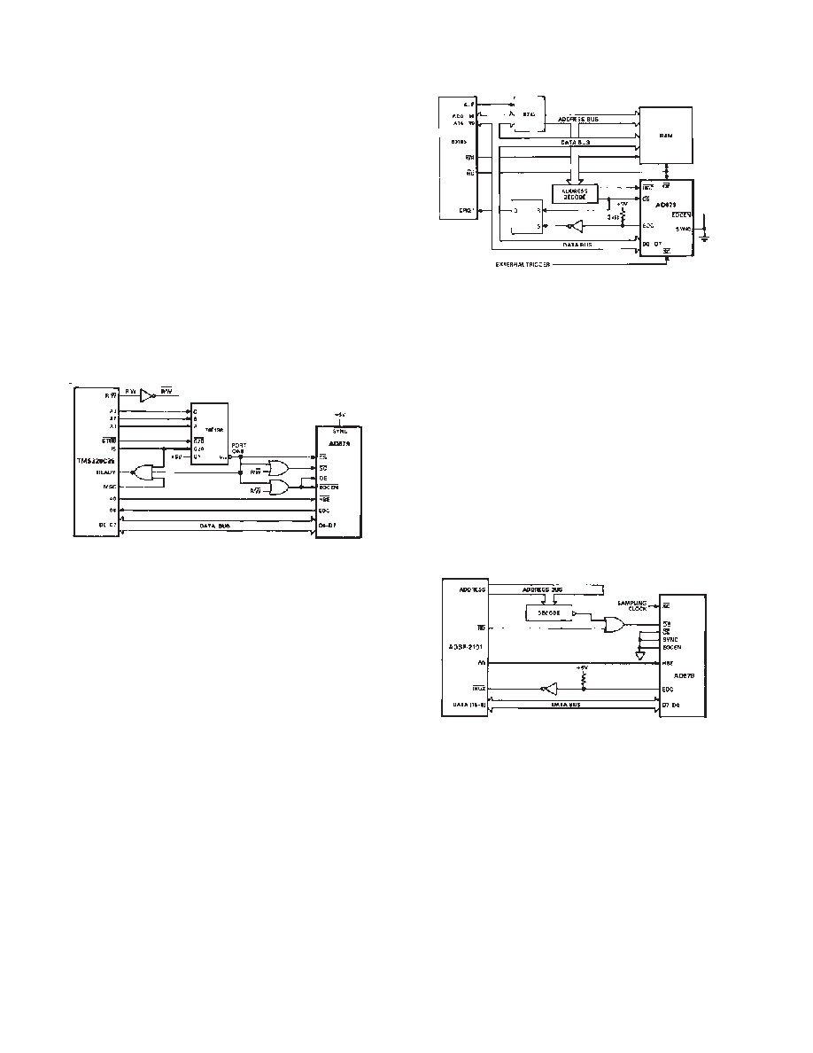
INTERFACING THE AD679 TO MICROPROCESSORS
The I/O capabilities of the AD679 allow direct interfacing to
general-purpose and DSP microprocessor buses. The asynchro-
nous conversion control feature allows complete flexibility and
control with minimal external hardware.
The following examples illustrate typical AD679 interface
configurations.
AD679 to TMS320C25
In Figure 9, the AD679 is mapped into the TMS320C25 I/O
space. AD679 conversions are initiated by issuing an OUT
instruction to Port 1. EOC status and the conversion result are
read in with an IN instruction to Port 1. A single wait state is
inserted by generating the processor READY input from
IS,
Port 1, and
MSC. Address line A0 provides HBE decoding to
select between the high and low bytes of data. This configura-
tion supports processor clock speeds of 20 MHz and is capable
of supporting processor clock speeds of 40 MHz if a NOP instruc-
tion follows each AD679 read instruction.
Figure 9. AD679 to TMS320C25 Interface
AD679 to 80186
Figure 10 shows the AD679 interfaced to the 80186 micropro-
cessor. This interface allows the 80186’s built-in DMA control-
ler to transfer the AD679 output into a RAM based FIFO buffer
of any length, with no microprocessor intervention.
In this application the AD679 is configured in the asynchronous
mode, which allows conversions to be initiated by an external
trigger source independent of the microprocessor clock. After
each conversion, the AD679 EOC signal generates a DMA
request to Channel 1 (DRQ1). The subsequent DMA READ
sequences the high and low byte AD679 data and resets the
interrupt latch. The system designer must assign a sufficient
priority to the DMA channel to ensure that the DMA request is
serviced before the next conversion is completed. This configu-
ration can be used with 6 MHz and 8 MHz 80186
processors.
Figure 10. AD679 to 80186 DMA Interface
AD679 to Analog Devices ADSP-2101
Figure 11 demonstrates the AD679 interfaced to an ADSP-2101.
With a clock frequency of 12.5 MHz, and instruction execution in
one 80 ns cycle, the digital signal processor supports the AD679
interface with one wait state.
The converter is configured to run asynchronously using a sam-
pling clock. The EOC output of the AD679 gets asserted at the
end of each conversion and causes an interrupt. Upon interrupt,
the ADSP-2101 immediately asserts its FO pin LOW. In the
following cycle, the processor starts a data memory read by pro-
viding an address on the DMA bus. The decoded address gener-
ates
OE for the converter, and the high byte of the conversion
result is read over the data bus. The read operation is extended
with one wait state and thus started and completed within two
processor cycles (160 ns). Next, the ADSP-2101 asserts its FO
HIGH. This allows the processor to start reading the lower byte
of data. This read operation executes in a similar manner to the
first and is completed during the next 160 ns.
Figure 11. AD679 to ADSP-2101 Interface
相关PDF资料 |
PDF描述 |
|---|---|
| AD7111BQ | IC DAC LOGARITHMIC 16-CDIP |
| AD7170BCPZ-REEL7 | IC ADC 12BIT SIGMA-DELTA 10LFCSP |
| AD7171BCPZ-REEL7 | IC ADC 16BIT SER 125HZ 10LFCSP |
| AD7190BRUZ-REEL | IC ADC 2CH 24BIT W/PGA 24TSSOP |
| AD7191BRUZ | IC ADC 2CH 24B SD 24TSSOP |
相关代理商/技术参数 |
参数描述 |
|---|---|
| AD679JD | 功能描述:IC ADC 14BIT SAMPLING 28-CDIP RoHS:否 类别:集成电路 (IC) >> 数据采集 - 模数转换器 系列:- 产品培训模块:Lead (SnPb) Finish for COTS Obsolescence Mitigation Program 标准包装:250 系列:- 位数:12 采样率(每秒):1.8M 数据接口:并联 转换器数目:1 功率耗散(最大):1.82W 电压电源:模拟和数字 工作温度:-40°C ~ 85°C 安装类型:表面贴装 封装/外壳:48-LQFP 供应商设备封装:48-LQFP(7x7) 包装:管件 输入数目和类型:2 个单端,单极 |
| AD679JN | 功能描述:IC ADC 14BIT 128KSPS 28-DIP RoHS:否 类别:集成电路 (IC) >> 数据采集 - 模数转换器 系列:- 标准包装:1 系列:- 位数:14 采样率(每秒):83k 数据接口:串行,并联 转换器数目:1 功率耗散(最大):95mW 电压电源:双 ± 工作温度:0°C ~ 70°C 安装类型:通孔 封装/外壳:28-DIP(0.600",15.24mm) 供应商设备封装:28-PDIP 包装:管件 输入数目和类型:1 个单端,双极 |
| AD679JNZ | 功能描述:IC ADC 14BIT 128KSPS 28-DIP RoHS:是 类别:集成电路 (IC) >> 数据采集 - 模数转换器 系列:- 其它有关文件:TSA1204 View All Specifications 标准包装:1 系列:- 位数:12 采样率(每秒):20M 数据接口:并联 转换器数目:2 功率耗散(最大):155mW 电压电源:模拟和数字 工作温度:-40°C ~ 85°C 安装类型:表面贴装 封装/外壳:48-TQFP 供应商设备封装:48-TQFP(7x7) 包装:Digi-Reel® 输入数目和类型:4 个单端,单极;2 个差分,单极 产品目录页面:1156 (CN2011-ZH PDF) 其它名称:497-5435-6 |
| AD679KD | 功能描述:IC ADC 14BIT SAMPLING 28-CDIP RoHS:否 类别:集成电路 (IC) >> 数据采集 - 模数转换器 系列:- 产品培训模块:Lead (SnPb) Finish for COTS Obsolescence Mitigation Program 标准包装:250 系列:- 位数:12 采样率(每秒):1.8M 数据接口:并联 转换器数目:1 功率耗散(最大):1.82W 电压电源:模拟和数字 工作温度:-40°C ~ 85°C 安装类型:表面贴装 封装/外壳:48-LQFP 供应商设备封装:48-LQFP(7x7) 包装:管件 输入数目和类型:2 个单端,单极 |
| AD679KN | 制造商:Analog Devices 功能描述:ADC Single Flash 128ksps 14-bit Parallel 28-Pin PDIP W |
发布紧急采购,3分钟左右您将得到回复。