- 您现在的位置:买卖IC网 > PDF目录20694 > AD680ANZ (Analog Devices Inc)IC VREF SERIES PREC 2.5V 8-PDIP PDF资料下载
参数资料
| 型号: | AD680ANZ |
| 厂商: | Analog Devices Inc |
| 文件页数: | 8/12页 |
| 文件大小: | 0K |
| 描述: | IC VREF SERIES PREC 2.5V 8-PDIP |
| 标准包装: | 50 |
| 基准类型: | 串联,精度 |
| 输出电压: | 2.5V |
| 容差: | ±0.2% |
| 温度系数: | 20ppm/°C |
| 输入电压: | 4.5 V ~ 36 V |
| 通道数: | 1 |
| 电流 - 静态: | 250µA |
| 工作温度: | -40°C ~ 85°C |
| 安装类型: | 通孔 |
| 封装/外壳: | 8-DIP(0.300",7.62mm) |
| 供应商设备封装: | 8-PDIP |
| 包装: | 管件 |
| 产品目录页面: | 795 (CN2011-ZH PDF) |
�� �
�
�AD680�
�+V� IN�
�TEMPERATURE� PERFORMANCE�
�0.1� μ� F�
�AD680�
�V� OUT�
�C� L�
�1000pF�
�V� L�
�V� OUT�
�249� Ω�
�V� OUT�
�0V�
�The� AD680� is� designed� for� reference� applications� where� tem-�
�perature� performance� is� important.� Extensive� temperature�
�testing� and� characterization� ensure� that� the� device’s� performance�
�is� maintained� over� the� specified� temperature� range.�
�Some� confusion� exists� in� the� area� of� defining� and� specifying�
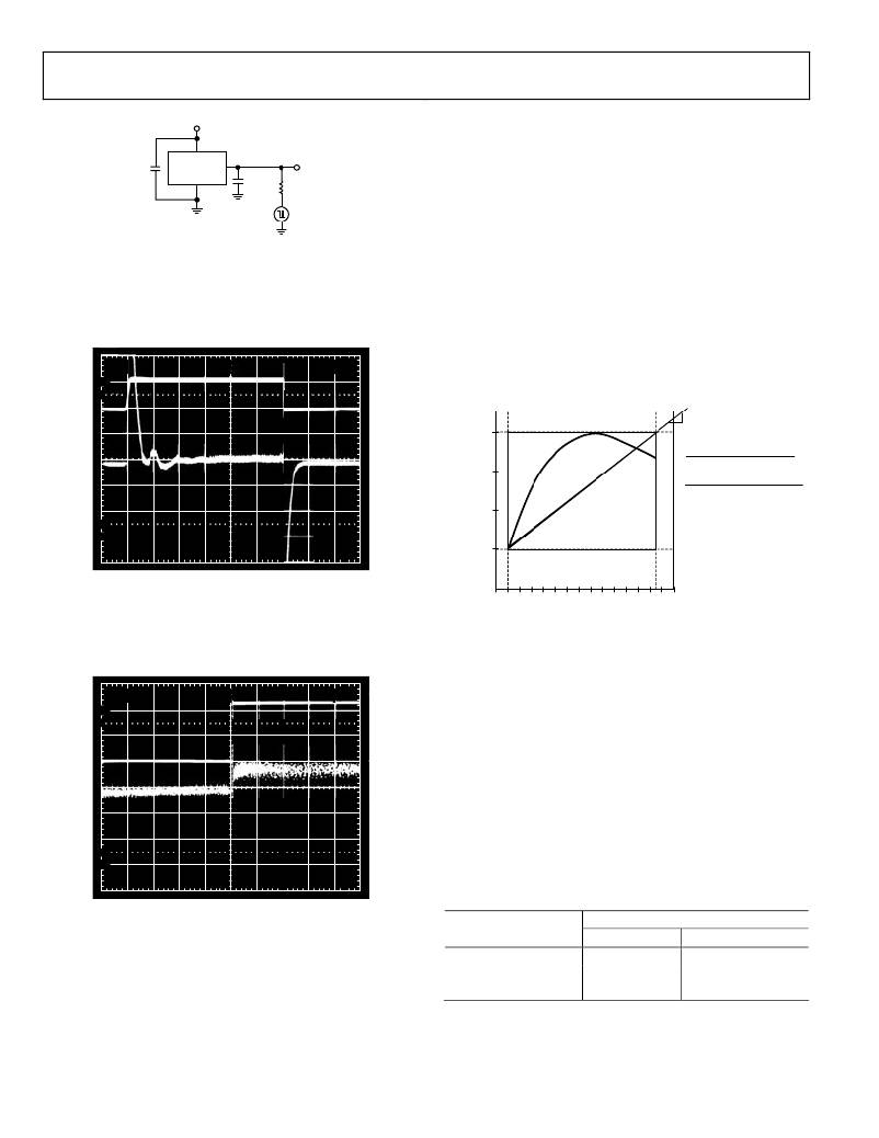
�Figure� 12.� Capacitive� Load� Transient� Response� Test� Circuit�
��1,000� pF,� 0� mA� to� 10� mA� load.�
�reference� voltage� error� over� temperature.� Historically,� references�
�have� been� characterized� using� a� maximum� deviation� per� degree�
�centigrade,� that� is,� ppm/°C.� However,� because� of� nonlinearities�
�in� temperature� characteristics� that� originated� in� standard� Zener�
�references� (such� as� “S”� type� characteristics),� most� manufac-�
�turers� now� use� a� maximum� limit� error� band� approach� to� specify�
�devices.� This� technique� involves� measuring� the� output� at� three�
�V� L�
�100�
�90�
�2V�
�5mV�
�5� μ� s�
�or� more� different� temperatures� to� specify� an� output� voltage�
�error� band.�
�2.501�
�SLOPE� =� TC�
�V� OUT�
�2.500�
�=�
�=�
�V� MAX� –� V� MIN�
�(T� MAX� –� T� MIN� )� ×� 2.5V� ×� 10� –6�
�2.501� –� 2.498�
�(85� °� C� –� (–40� °� C))� ×� 2.5V� ×� 10� –6�
�10�
�0%�
�2.499�
�2.498�
�=� 9.6ppm/� °� C�
�Figure� 13.� Output� Response� with� Capacitive� Load�
�–50�
�–30�
�–10� 0� 20� 40�
�60�
�80�
�100�
�LOAD� REGULATION�
��the� AD680.�
�TEMPERATURE� (� °� C)�
�Figure� 15.� Typical� AD680AN/AD680AR� Temperature� Drift�
��AD680AR� and� illustrates� the� test� methodology.� The� box� in�
�V� L�
�100�
�90�
�1V�
�1mV�
�100� μ� s�
��ing� temperature� extremes,� and� on� the� top� and� bottom� by� the�
�maximum� and� minimum� output� voltages� measured� over� the�
�operating� temperature� range.�
�The� maximum� height� of� the� box� for� the� appropriate� temperature�
�V� OUT�
�10�
�0%�
�Figure� 14.� Typical� Load� Regulation� Characteristics�
�range� and� device� grade� is� shown� in� Table� 4.� Duplication� of� these�
�results� requires� a� combination� of� high� accuracy� and� stable� tem-�
�perature� control� in� a� test� system.� Evaluation� of� the� AD680� will�
�produce� a� curve� similar� to� that� in� Figure� 15,� but� output� readings�
�could� vary� depending� upon� the� test� equipment� used.�
�Table� 4.� Maximum� Output� Change� in� mV�
�Maximum� Output� Change� (mV)�
�Device� Grade�
�AD680JN/AD680JR�
�AD680JT�
�AD680AN�
�Rev.� H� |� Page� 8� of� 12�
�0°C� to� 70°C�
�4.375�
�5.250�
�Not� applicable�
�?40°C� to� +85°C�
�Not� applicable�
�Not� applicable�
�6.250�
�相关PDF资料 |
PDF描述 |
|---|---|
| VE-JNW-CX-F2 | CONVERTER MOD DC/DC 5.5V 75W |
| EEC12DRTN-S93 | CONN EDGECARD 24POS DIP .100 SLD |
| ACB35DHAS | CONN EDGECARD 70POS R/A .050 DIP |
| EMM36DTMT-S273 | CONN EDGECARD 72POS R/A .156 SLD |
| EMM36DTBT-S273 | CONN EDGECARD 72POS R/A .156 SLD |
相关代理商/技术参数 |
参数描述 |
|---|---|
| AD680ANZ | 制造商:Analog Devices 功能描述:IC, SERIES V-REF, 2.5V, 5mV, 8-DIP |
| AD680ANZ1 | 制造商:AD 制造商全称:Analog Devices 功能描述:Low Power, Low Cost 2.5 V Reference |
| AD680AR | 制造商:Analog Devices 功能描述:V-Ref Precision 2.5V 10mA 8-Pin SOIC N Tube 制造商:Analog Devices 功能描述:Voltage Regulator IC Output Voltage Max. |
| AD680AR-REEL | 制造商:Analog Devices 功能描述:V-Ref Precision 2.5V 10mA 8-Pin SOIC N T/R |
| AD680AR-REEL7 | 制造商:Analog Devices 功能描述:V-Ref Precision 2.5V 10mA 8-Pin SOIC N T/R 制造商:Rochester Electronics LLC 功能描述:IC, 2.5V REFERENCE - Tape and Reel |
发布紧急采购,3分钟左右您将得到回复。