- 您现在的位置:买卖IC网 > PDF目录11674 > AD693AD (Analog Devices Inc)IC SGNL COND 4-20MA TX 20-CDIP PDF资料下载
参数资料
| 型号: | AD693AD |
| 厂商: | Analog Devices Inc |
| 文件页数: | 3/12页 |
| 文件大小: | 0K |
| 描述: | IC SGNL COND 4-20MA TX 20-CDIP |
| 标准包装: | 19 |
| 类型: | 信号调节器 |
| 输入类型: | 电压 |
| 输出类型: | 电压 |
| 接口: | 3 线 |
| 电流 - 电源: | 20mA |
| 安装类型: | 通孔 |
| 封装/外壳: | 20-CDIP(0.300",7.62mm) |
| 供应商设备封装: | 20-CDIP |
| 包装: | 管件 |
| 产品目录页面: | 798 (CN2011-ZH PDF) |
AD693
REV. A
–11–
Table II. Thermocouple Application—Cold Junction Compensation
30 mV
60 mV
AMBIENT
TEMP
POLARITY
MATERIAL
TYPE
TEMP
RCOMP
RZ
RANGE
+
IRON
J
25
°
51.7
301K
546
°C
1035
°C
–
CONSTANTAN
75
°
53.6
294K
+
NICKEL-CHROME
25
°
40.2
392K
721
°C—
_
NICKEL-ALUMINUM
K
75
°
42.2
374K
+
NICKEL-CHROME
25
°
60.4
261K
E
413
°C
787
°C
–
COPPER-NICKEL
75
°
64.9
243K
+
COPPER
25
°
40.2
392K
T
USE WITH GAIN >2
–
COPPER-NICKEL
75
°
45.3
340K
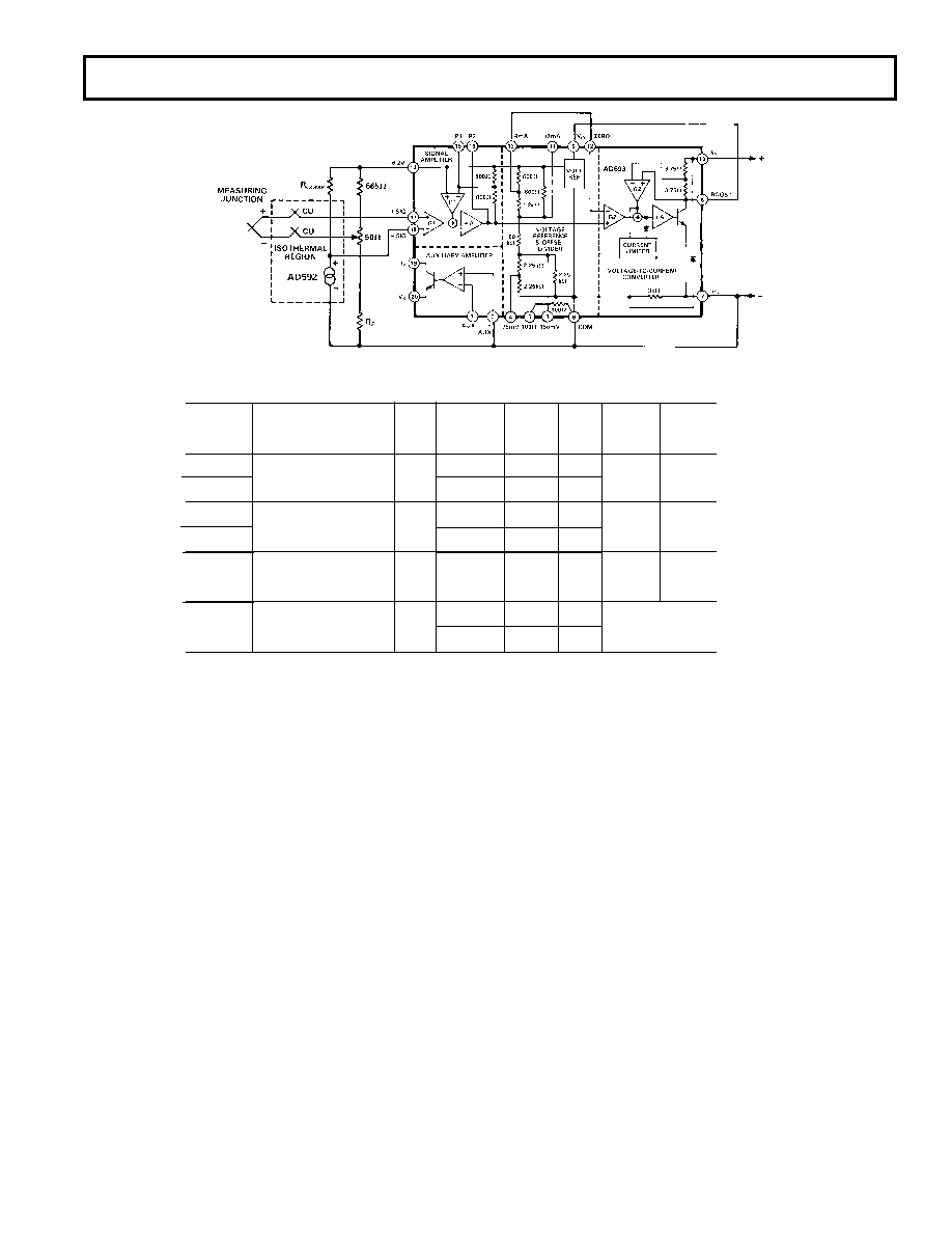
Figure 19. Thermocouple Inputs with Cold Junction Compensation
Table III lists the expressions required to calculate the total
error. The AD693 is tested with a 250
load, a 24 V loop supply
Table III. RTI Contributions to Span and Offset Error
RTI Contributions to Offset Error
Error Source
Expression for RTI Error at Zero
IZE
Zero Current Error
IZE/XS
PSRR
Power Supply Rejection Ratio
(|VLOOP – 24 V| + [|RL – 250 | × IZ]) × PSRR
CMRR Common-Mode Rejection Ratio |VCM – 3.1 V| × CMRR
IOS
Input Offset Current
RS
× IOS
RTI Contributions to Span Error
Error Source
Expression for RTI Error at Full Scale
XSE
Transconductance Error
VSPAN
× X
SE
XPSRR
Transconductance PSRR
1
|RL – 250 | × IS × PSRR
XCMRR Transconductance CMRR
|VCM – 3.1 V| × VSPAN × XCMRR
XNL
Nonlinearity
VSPAN
× X
NL
IDIFF
Differential Input Current
2
RS
× I
DIFF
Abbreviations
IZ
Zero Current (usually 4 mA)
IS
Output span (usually 16 mA)
RS
Input source impedance
RL
Load resistance
VLOOP Loop supply voltage
VCM
Input common-mode voltage
VSPAN
Input span
XS
Nominal transconductance in A/V
1The 4–20 mA signal, flowing through the metering resistor, modulates the power supplyvoltage seen
by the AD693. The change in voltage causes a power supply rejection error that varies with the
output current, thus it appears as a span error.
2The input bias current of the inverting input increases with input signal voltage. The differential
input current, IDIFF, equals the inverting input current minus the noninverting input current; see
Figure 2. IDIFF, flowing into an input source impedance, will cause an input voltage error that var-
ies with signal. If the change in differential input current with input signal is approximated as a
linear function, then any error due to source impedance may be approximated as a span error. To
calculate IDIFF, refer to Figure 2 and find the value for IDIFF/ + In corresponding to the full-scale
input voltage for your application. Multiply by + In max to get IDlFF. Multiply IDIFF by the source
impedance to get the input voltage error at full scale.
via a set of thermocouple tables referenced to
°C. For example,
the output of a properly referenced type J thermocouple is
60 mV when the hot junction is at 1035
°C. Table II lists the
maximum measurement temperature for several thermocouple
types using the preadjusted 30 mV and 60 mV input ranges.
More convenient temperature ranges can be selected by deter-
mining the full-scale input voltages via standard thermocouple
tables and adjusting the AD693 span. For example, suppose
only a 300
°C span is to be measured with a type K thermo-
couple. From a standard table, the thermocouple output is
12.207 mV; since 60 mV at the signal amplifier corresponds to a
16 mA span at the output a gain of 5, or more precisely 60 mV/
12.207 mV = 4.915 will be needed. Using a 12.207 mV span in
the gain resistor formula given in “Adjusting Input Span” yields
a value of about 270
as the minimum from P1 to 6.2 V. Adding
a 50
potentiometer will allow ample adjustment range.
With the connection illustrated, the AD693 will give a full-scale
indication with an open thermocouple.
ERROR BUDGET ANALYSIS
Loop-Powered Operation specifications refer to parameters
tested with the AD693 operating as a loop-powered transmitter.
The specifications are valid for the preset spans of 30 mV,
60 mV and those spans in between. The section, “Components
of Error,” refers to parameters tested on the individual functional
blocks, (Signal Amplifier, V/I Converter, Voltage Reference, and
Auxiliary Amplifier). These can be used to get an indication of
device performance when the AD693 is used in local power
mode or when it is adjusted to spans of less than 30 mV.
相关PDF资料 |
PDF描述 |
|---|---|
| AD9824KCPZ | IC CCD SIGNAL PROC 14BIT 48LFCSP |
| AD9979BCPZ | IC PROCESSOR CCD 14BIT 48-LFCSP |
| AD694BRZ | IC TRANSMITTER 4-20MA 16-SOIC |
| LTK001ACN8#PBF | IC THERMOCOUPL COMP& KIT 8DIP |
| AD693AQ | IC TRANSMITTER 4-20MA 20-CDIP |
相关代理商/技术参数 |
参数描述 |
|---|---|
| AD693AE | 功能描述:IC SGNL COND 4-20MA TX 20-CLCC RoHS:否 类别:集成电路 (IC) >> 接口 - 传感器和探测器接口 系列:- 其它有关文件:Automotive Product Guide 产品培训模块:Lead (SnPb) Finish for COTS Obsolescence Mitigation Program 标准包装:74 系列:- 类型:触控式传感器 输入类型:数字 输出类型:数字 接口:JTAG,串行 电流 - 电源:100µA 安装类型:表面贴装 封装/外壳:20-TSSOP(0.173",4.40mm 宽) 供应商设备封装:20-TSSOP 包装:管件 |
| AD693AQ | 功能描述:IC TRANSMITTER 4-20MA 20-CDIP RoHS:否 类别:集成电路 (IC) >> 接口 - 传感器和探测器接口 系列:- 其它有关文件:Automotive Product Guide 产品培训模块:Lead (SnPb) Finish for COTS Obsolescence Mitigation Program 标准包装:74 系列:- 类型:触控式传感器 输入类型:数字 输出类型:数字 接口:JTAG,串行 电流 - 电源:100µA 安装类型:表面贴装 封装/外壳:20-TSSOP(0.173",4.40mm 宽) 供应商设备封装:20-TSSOP 包装:管件 |
| AD693BQ | 制造商:AD 制造商全称:Analog Devices 功能描述:Loop-Powered 4a??20 mA Sensor Transmitter |
| AD694 | 制造商:AD 制造商全称:Analog Devices 功能描述:4.20 mA Transmitter |
发布紧急采购,3分钟左右您将得到回复。