参数资料
| 型号: | AD698AP |
| 厂商: | Analog Devices Inc |
| 文件页数: | 10/12页 |
| 文件大小: | 0K |
| 描述: | IC LVDT SIGNAL COND 28-PLCC |
| 标准包装: | 1 |
| 类型: | 信号调节器 |
| 输入类型: | 电压 |
| 输出类型: | 电压 |
| 接口: | LVDT |
| 电流 - 电源: | 15mA |
| 安装类型: | 表面贴装 |
| 封装/外壳: | 28-LCC(J 形引线) |
| 供应商设备封装: | 28-PLCC(11.51x11.51) |
| 包装: | 管件 |
AD698
REV. B
–7–
b. Full-scale core displacement from null, d
S
× d = VTR and also equals the ratio A/B at mechanical full
scale. The VTR should be converted to units of V/V.
For a full-scale displacement of d inches, voltage out of the
AD698 is computed as
VOUT = S
× d × 500 A × R2
VOUT is measured with respect to the signal reference,
Pin 21, shown in Figure 7.
Solving for R2,
R2
=
VOUT
S
× d × 500 A
(1)
For VOUT =
±10 V full-scale range (20 V span) and d = ±0.1
inch full-scale displacement (0.2 inch span)
R2
=
20V
2.4
× 0.2 × 500 A =
83. 3 k
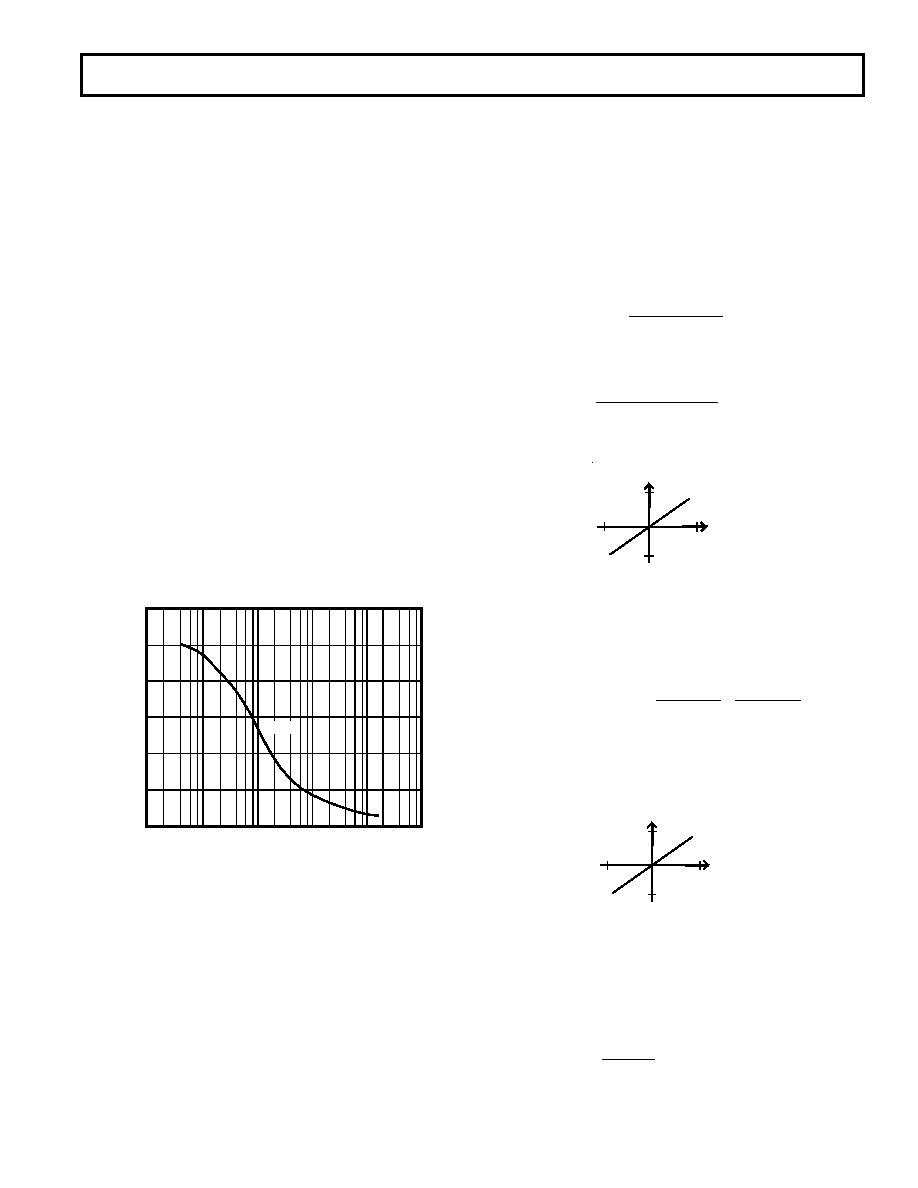
VOUT as a function of displacement for the above example is
shown in Figure 10.
+10
+0.1d (INCHES)
–0.1
–10
V
OUT
(VOLTS)
Figure 10. VOUT (
±10 V Full Scale) vs. Core Displace-
ment (
±0.1 Inch)
E. Optional Offset of Output Voltage Swing
9. Selections of R3 and R4 permit a positive or negative output
voltage offset adjustment.
VOS = 1.2 V × R2 ×
1
R3
+ 2 k
–
1
R4
+ 2 k
(2)
For no offset adjustment R3 and R4 should be open circuit.
To design a circuit producing a 0 V to +10 V output for a
displacement of +0.1 inch, set VOUT to +10 V, d = 0.2 inch
and solve Equation (1) for R2.
+5
+0.1d (INCHES)
–0.1
–5
V
OUT
(VOLTS)
Figure 11. VOUT (±5 V Full Scale) vs. Core Displacement
(
±0.1 Inch)
This will produce a response shown in Figure 11.
In Equation (2) set VOS = 5 V and solve for R3 and R4. Since a
positive offset is desired, let R4 be open circuit. Rearranging
Equation (2) and solving for R3
R3
= 1.2 × R2
VOS
–2 k
= 7.02 k
Multiply the primary excitation voltage by the VTR to get
the expected secondary voltage at mechanical full scale. For
example, for an LVDT with a sensitivity of 2.4 mV/V/mil and
a full scale of
±0.1 inch, the VTR = 0.0024 V/V/Mil × 100
mil = 0.24. Assuming the maximum excitation of 3.5 V rms,
the maximum secondary voltage will be 3.5 V rms
× 0.24 =
0.84 V rms, which is in the acceptable range.
Conversely the VTR may be measured explicitly. With the
LVDT energized at its typical drive level VPRI, as indicated
by the manufacturer, set the core displacement to its me-
chanical full-scale position and measure the output VSEC of
the secondary. Compute the LVDT voltage transformation
ratio, VTR. VTR = VSEC//VPRI. For the E100, VSEC = 0.72 V
for VPRI = 3 V. VTR = 0.24.
For situations where LVDT sensitivity is low, or the me-
chanical FS is a small fraction of the total stroke length, an
input excitation of more than 3.5 V rms may be needed. In
this case a voltage divider network may be placed across the
LVDT primary to provide smaller voltage for the +BIN and
–BIN input. If, for example, a network was added to divide
the B Channel input by 1/2, then the VTR should also be re-
duced by 1/2 for the purpose of component selection.
Check the power supply voltages by verifying that the peak
values of VA and VB are at least 2.5 volts less than the volt-
ages at +VS and –VS.
6. Referring to Figure 9, for VS = ± 15 V, select the value of the
amplitude determining component R1 as shown by the curve
in Figure 9.
30
15
0
0.01
0.1
1k
100
10
1
5
10
20
25
V rms
R1 – k
V
EXC
–
V
rm
s
Figure 9. Excitation Voltage VEXC vs. R1
7. C2, C3 and C4 are a function of the desired bandwidth of
the AD698 position measurement subsystem. They should
be nominally equal values.
C2 = C3 = C4 = 10
–4 Farad Hz/f
5UBSYSTEM (Hz)
If the desired system bandwidth is 250 Hz, then
C2 = C3 = C4 = 10
-4 Farad Hz/250 Hz = 0.4
F
See Figures 14, 15 and 16 for more information about
AD698 bandwidth and phase characterization.
D. Set the Full-Scale Output Voltage
8. To compute R2, which sets the AD698 gain or full-scale
output range, several pieces of information are needed:
a. LVDT sensitivity, S
相关PDF资料 |
PDF描述 |
|---|---|
| AD7142ACPZ-500RL7 | IC CAP-TO-DGTL CONV PROG 32LFCSP |
| AD7143ACPZ-1REEL | IC CONV CAP-TO-DGTL PROG 16LFCSP |
| AD7147A-1ACBZ500R7 | IC CDC 13CH I2C W/RAM 25WLCSP |
| AD7147WPACPZ-1500R | IC CAP-TO-DGTL CONV PROG 24LFCSP |
| AD7150BRMZ-REEL | IC CAP CONV 2CH ULT LP 10MSOP |
相关代理商/技术参数 |
参数描述 |
|---|---|
| AD698APZ | 功能描述:IC LVDT SIGNAL COND 28-PLCC RoHS:是 类别:集成电路 (IC) >> 接口 - 传感器和探测器接口 系列:- 其它有关文件:Automotive Product Guide 产品培训模块:Lead (SnPb) Finish for COTS Obsolescence Mitigation Program 标准包装:74 系列:- 类型:触控式传感器 输入类型:数字 输出类型:数字 接口:JTAG,串行 电流 - 电源:100µA 安装类型:表面贴装 封装/外壳:20-TSSOP(0.173",4.40mm 宽) 供应商设备封装:20-TSSOP 包装:管件 |
| AD698APZ | 制造商:Analog Devices 功能描述:IC LVDT SIGNAL COND 28PLCC 制造商:Analog Devices 功能描述:IC, LVDT SIGNAL COND, 28PLCC |
| AD698APZ | 制造商:Analog Devices 功能描述:IC, LVDT SIGNAL COND, 20KHZ, 0.05% LCC28 |
| AD698SQ | 功能描述:IC LVDT SGNL COND UNVRSL 24CDIP RoHS:否 类别:集成电路 (IC) >> 接口 - 传感器和探测器接口 系列:- 其它有关文件:Automotive Product Guide 产品培训模块:Lead (SnPb) Finish for COTS Obsolescence Mitigation Program 标准包装:74 系列:- 类型:触控式传感器 输入类型:数字 输出类型:数字 接口:JTAG,串行 电流 - 电源:100µA 安装类型:表面贴装 封装/外壳:20-TSSOP(0.173",4.40mm 宽) 供应商设备封装:20-TSSOP 包装:管件 |
| AD-6B | 制造商:Altas 功能描述: |
发布紧急采购,3分钟左右您将得到回复。