- 您现在的位置:买卖IC网 > PDF目录165342 > AD711JNZ (ANALOG DEVICES INC) Precision, Low Cost, High Speed, BiFET Op Amp PDF资料下载
参数资料
| 型号: | AD711JNZ |
| 厂商: | ANALOG DEVICES INC |
| 元件分类: | 运算放大器 |
| 英文描述: | Precision, Low Cost, High Speed, BiFET Op Amp |
| 中文描述: | OP-AMP, 3000 uV OFFSET-MAX, 4 MHz BAND WIDTH, PDIP8 |
| 封装: | MINI, PLASTIC, DIP-8 |
| 文件页数: | 14/16页 |
| 文件大小: | 711K |
| 代理商: | AD711JNZ |
REV. E
AD711
–7–
OPTIMIZING SETTLING TIME
Most bipolar high-speed D/A converters have current outputs;
therefore, for most applications, an external op amp is required
for current-to-voltage conversion. The settling time of the
converter/op amp combination depends on the settling time of
the DAC and output amplifier. A good approximation is:
t
S Total
= (t
S DAC )
2
+(t
S AMP )
2
(1)
The settling time of an op amp DAC buffer will vary with the
noise gain of the circuit, the DAC output capacitance, and with
the amount of external compensation capacitance across the
DAC output scaling resistor.
Settling time for a bipolar DAC is typically 100 ns to 500 ns.
Previously, conventional op amps have required much longer
settling times than have typical state-of-the-art DACs; therefore,
the amplifier settling time has been the major limitation to a
high-speed voltage-output D-to-A function. The introduction
of the AD711/712 family of op amps with their 1
ms (to ±0.01%
of final value) settling time now permits the full high-speed
capabilities of most modern DACs to be realized.
In addition to a significant improvement in settling time, the
low offset voltage, low offset voltage drift, and high open-loop
gain of the AD711 family assures 12-bit accuracy over the full
operating temperature range.
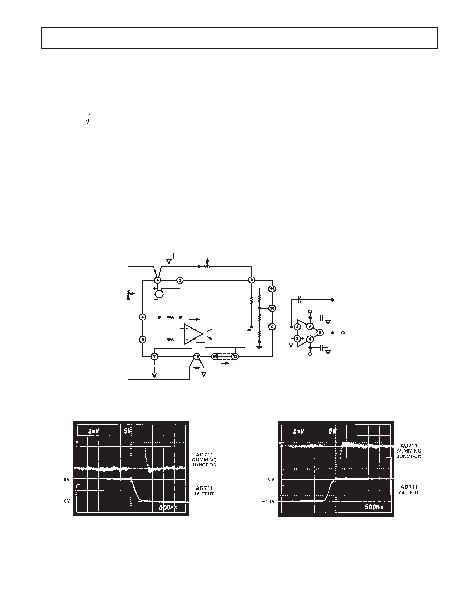
The excellent high-speed performance of the AD711 is shown
in the oscilloscope photos of Figure 2. Measurements were taken
using a low input capacitance amplifier connected directly to the
summing junction of the AD711 – both photos show the worst
case situation: a full-scale input transition. The DAC’s 4 k
W
[10 k
W 8 kW = 4.4 kW] output impedance together with a 10 kW
feedback resistor produce an op amp noise gain of 3.25. The
current output from the DAC produces a 10 V step at the op
amp output (0 to –10 V Figure 2a, –10 V to 0 V Figure 2b.)
Therefore, with an ideal op amp, settling to
±1/2 LSB (±0.01%)
requires that 375
mV or less appears at the summing junction.
This means that the error between the input and output (that
voltage which appears at the AD711 summing junction) must
be less than 375
mV. As shown in Figure 2, the total settling time
for the AD711/AD565 combination is 1.2 microseconds.
OUTPUT
–10V TO +10V
+15V
0.1 F
10pF
0.1 F
AD711K
DAC
IOUT = 4
IREF
CODE
0.5mA
IREF
20k
19.95k
R1
100
BIPOLAR
OFFSET ADJUST
IO
DAC
OUT
10V
SPAN
–15V
20V
SPAN
5k
10V
MSB
LSB
REF
OUT
VCC
REF
IN
REF
GND
R2
100
GAIN
ADJUST
0.1 F
AD565A
BIPOLAR
OFF
9.95k
–VEE
0.1 F
POWER
GND
Figure 1.
±10 V Voltage Output Bipolar DAC
Figure 2. Settling Characteristics for AD711 with AD565A
a. (Full-Scale Negative Transition)
b. (Full-Scale Positive Transition)
相关PDF资料 |
PDF描述 |
|---|---|
| AD711JRZ | Precision, Low Cost, High Speed, BiFET Op Amp |
| AD711KNZ | Precision, Low Cost, High Speed, BiFET Op Amp |
| AD711KRZ | Precision, Low Cost, High Speed, BiFET Op Amp |
| AD713JNZ | Quad Precision, Low Cost, High Speed, BiFET Op Amp |
| AD713JRZ-16 | Quad Precision, Low Cost, High Speed, BiFET Op Amp |
相关代理商/技术参数 |
参数描述 |
|---|---|
| AD711JR | 功能描述:IC OPAMP BIFET PREC 25MA 8SOIC RoHS:否 类别:集成电路 (IC) >> Linear - Amplifiers - Instrumentation 系列:- 其它有关文件:Automotive Product Guide 产品培训模块:Lead (SnPb) Finish for COTS Obsolescence Mitigation Program 标准包装:1 系列:- 放大器类型:通用 电路数:1 输出类型:满摆幅 转换速率:3 V/µs 增益带宽积:10MHz -3db带宽:- 电流 - 输入偏压:1pA 电压 - 输入偏移:70µV 电流 - 电源:2.5mA 电流 - 输出 / 通道:48mA 电压 - 电源,单路/双路(±):2.7 V ~ 5.5 V,±1.35 V ~ 2.75 V 工作温度:-40°C ~ 125°C 安装类型:表面贴装 封装/外壳:SOT-23-6 供应商设备封装:SOT-6 包装:Digi-Reel® 其它名称:MAX4475AUT#TG16DKR |
| AD711JR-REEL | 功能描述:IC OPAMP BIFET PREC 25MA 8SOIC RoHS:否 类别:集成电路 (IC) >> Linear - Amplifiers - Instrumentation 系列:- 标准包装:1,000 系列:- 放大器类型:电压反馈 电路数:4 输出类型:满摆幅 转换速率:33 V/µs 增益带宽积:20MHz -3db带宽:30MHz 电流 - 输入偏压:2nA 电压 - 输入偏移:3000µV 电流 - 电源:2.5mA 电流 - 输出 / 通道:30mA 电压 - 电源,单路/双路(±):4.5 V ~ 16.5 V,±2.25 V ~ 8.25 V 工作温度:-40°C ~ 85°C 安装类型:表面贴装 封装/外壳:14-SOIC(0.154",3.90mm 宽) 供应商设备封装:14-SOIC 包装:带卷 (TR) |
| AD711JR-REEL7 | 功能描述:IC OPAMP BIFET PREC 25MA 8SOIC RoHS:否 类别:集成电路 (IC) >> Linear - Amplifiers - Instrumentation 系列:- 标准包装:1,000 系列:- 放大器类型:电压反馈 电路数:4 输出类型:满摆幅 转换速率:33 V/µs 增益带宽积:20MHz -3db带宽:30MHz 电流 - 输入偏压:2nA 电压 - 输入偏移:3000µV 电流 - 电源:2.5mA 电流 - 输出 / 通道:30mA 电压 - 电源,单路/双路(±):4.5 V ~ 16.5 V,±2.25 V ~ 8.25 V 工作温度:-40°C ~ 85°C 安装类型:表面贴装 封装/外壳:14-SOIC(0.154",3.90mm 宽) 供应商设备封装:14-SOIC 包装:带卷 (TR) |
| AD711JRZ | 功能描述:IC OPAMP BIFET PREC 25MA 8SOIC RoHS:是 类别:集成电路 (IC) >> Linear - Amplifiers - Instrumentation 系列:- 产品培训模块:Differential Circuit Design Techniques for Communication Applications 标准包装:1 系列:- 放大器类型:RF/IF 差分 电路数:1 输出类型:差分 转换速率:9800 V/µs 增益带宽积:- -3db带宽:2.9GHz 电流 - 输入偏压:3µA 电压 - 输入偏移:- 电流 - 电源:40mA 电流 - 输出 / 通道:- 电压 - 电源,单路/双路(±):3 V ~ 3.6 V 工作温度:-40°C ~ 85°C 安装类型:表面贴装 封装/外壳:16-VQFN 裸露焊盘,CSP 供应商设备封装:16-LFCSP-VQ 包装:剪切带 (CT) 产品目录页面:551 (CN2011-ZH PDF) 其它名称:ADL5561ACPZ-R7CT |
| AD711JRZ-REEL | 功能描述:IC OPAMP BIFET PREC 25MA 8SOIC RoHS:是 类别:集成电路 (IC) >> Linear - Amplifiers - Instrumentation 系列:- 标准包装:2,500 系列:- 放大器类型:通用 电路数:1 输出类型:满摆幅 转换速率:0.11 V/µs 增益带宽积:350kHz -3db带宽:- 电流 - 输入偏压:4nA 电压 - 输入偏移:20µV 电流 - 电源:260µA 电流 - 输出 / 通道:20mA 电压 - 电源,单路/双路(±):2.7 V ~ 36 V,±1.35 V ~ 18 V 工作温度:-40°C ~ 85°C 安装类型:表面贴装 封装/外壳:8-SOIC(0.154",3.90mm 宽) 供应商设备封装:8-SO 包装:带卷 (TR) |
发布紧急采购,3分钟左右您将得到回复。