参数资料
| 型号: | AD712JR-REEL |
| 厂商: | Analog Devices Inc |
| 文件页数: | 4/20页 |
| 文件大小: | 0K |
| 描述: | IC OPAMP BIFET DUAL PREC 8SOIC |
| 标准包装: | 2,500 |
| 放大器类型: | J-FET |
| 电路数: | 2 |
| 转换速率: | 20 V/µs |
| -3db带宽: | 4MHz |
| 电流 - 输入偏压: | 25pA |
| 电压 - 输入偏移: | 300µV |
| 电流 - 电源: | 5mA |
| 电流 - 输出 / 通道: | 25mA |
| 电压 - 电源,单路/双路(±): | 9 V ~ 36 V,±4.5 V ~ 20 V |
| 工作温度: | 0°C ~ 70°C |
| 安装类型: | 表面贴装 |
| 封装/外壳: | 8-SOIC(0.154",3.90mm 宽) |
| 供应商设备封装: | 8-SO |
| 包装: | 带卷 (TR) |
AD712
Rev. H | Page 12 of 20
OP AMP SETTLING TIME—A MATHEMATICAL
MODEL
The design of the AD712 gives careful attention to optimizing
individual circuit components; in addition, a careful trade-off
was made: the gain bandwidth product (4 MHz) and slew rate
(20 V/μs) were chosen to be high enough to provide very fast
settling time but not too high to cause a significant reduction
in phase margin (and therefore, stability). Thus designed, the
AD712 settles to ±0.01%, with a 10 V output step, in under 1 μs,
while retaining the ability to drive a 250 pF load capacitance
when operating as a unity-gain follower.
If an op amp is modeled as an ideal integrator with a unity-gain
crossover frequency of ωO/2π, then Equation 1 accurately
describes the small signal behavior of the circuit of Figure 32,
consisting of an op amp connected as an I-to-V converter at the
output of a bipolar or CMOS DAC. This equation would com-
pletely describe the output of the system if not for the finite slew
rate and other nonlinear effects of the op amp.
1
)
(
2
+
+
ω
+
ω
=
s
RC
G
s
C
R
I
V
f
O
N
O
X
IN
O
(1)
Where
π
ω
2
O = unity-gain frequency of the op amp.
GN = noise gain of circuit
+
O
R
1
.
This equation can then be solved for Cf
(
)
2
1
2
O
N
O
X
O
N
X
R
G
RC
R
G
C
ω
+
ω
+
ω
=
(2)
In these equations, Capacitance CX is the total capacitance
appearing at the inverting terminal of the op amp. When
modeling a DAC buffer application, the Norton equivalent
circuit shown in Figure 32 can be used directly; Capacitance CX
is the total capacitance of the output of the DAC plus the input
capacitance of the op amp (because the two are in parallel).
VOUT
RL
CL
CF
R
IO
RO
CX
1/2
AD712
+
–
0
082
3-
0
32
Figure 32. Simplified Model of the AD712 Used as a Current-Out DAC Buffer
When RO and IO are replaced with their Thevenin VIN and RIN
equivalents, the general-purpose inverting amplifier shown in
Figure 33 is created. Note that when using this general model,
Capacitance CX is either the input capacitance of the op amp, if
a simple inverting op amp is being simulated, or the combined
capacitance of the DAC output and the op amp input if the
DAC buffer is being modeled.
VOUT
RL
CL
CF
R
VIN
RIN
CX
1/2
AD712
+
–
00
82
3-
03
3
Figure 33. Simplified Model of the AD712 Used as an Inverter
In either case, Capacitance CX causes the system to go from a
one-pole to a two-pole response; this additional pole increases
settling time by introducing peaking or ringing in the op amp
output. Because the value of CX can be estimated with reasonable
accuracy, Equation 2 can be used to choose a small capacitor
(CF) to cancel the input pole and optimize amplifier response.
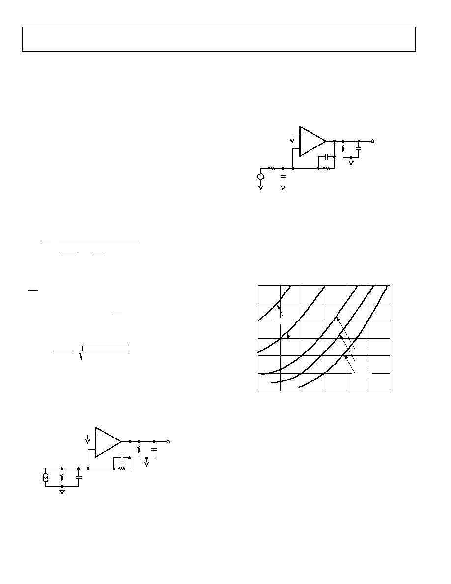
Figure 34 is a graphical solution of Equation 2 for the AD712
with R = 4 kΩ.
CF
C
X
40
30
0
10
0
20
10
50
60
GN = 4.0
GN = 3.0
20
30
40
50
60
GN = 2.0
GN = 1.5
GN = 1.0
00
82
3-
03
4
Figure 34. Value of Capacitor CF vs. Value of CX
相关PDF资料 |
PDF描述 |
|---|---|
| NPTC331KFXC-RC | CONN FEMALE 33POS .1" SMD TIN |
| TA45-A144F060C0 | CIRCUIT BRKR THERMAL 6A 2POLE |
| 953408-6602-AR | CONN SOCKET 8POS 2MM VERT T/H |
| 5-1879213-1 | RES 88.7 OHM 1/16W 0.1% 0402 |
| PPTC222LJBN-RC | CONN FEMALE 44POS DL .1" R/A TIN |
相关代理商/技术参数 |
参数描述 |
|---|---|
| AD712JR-REEL7 | 功能描述:IC OPAMP BIFET DUAL PREC 8SOIC RoHS:否 类别:集成电路 (IC) >> Linear - Amplifiers - Instrumentation 系列:- 标准包装:1 系列:- 放大器类型:通用 电路数:4 输出类型:满摆幅 转换速率:0.6 V/µs 增益带宽积:1MHz -3db带宽:- 电流 - 输入偏压:2pA 电压 - 输入偏移:1000µV 电流 - 电源:85µA 电流 - 输出 / 通道:20mA 电压 - 电源,单路/双路(±):1.8 V ~ 6 V 工作温度:-40°C ~ 125°C 安装类型:表面贴装 封装/外壳:14-SOIC(0.154",3.90mm 宽) 供应商设备封装:14-SOICN 包装:剪切带 (CT) 产品目录页面:680 (CN2011-ZH PDF) 其它名称:MCP6L04T-E/SLCT |
| AD712JRZ | 功能描述:IC OPAMP BIFET DUAL PREC 8SOIC RoHS:是 类别:集成电路 (IC) >> Linear - Amplifiers - Instrumentation 系列:- 产品培训模块:Differential Circuit Design Techniques for Communication Applications 标准包装:1 系列:- 放大器类型:RF/IF 差分 电路数:1 输出类型:差分 转换速率:9800 V/µs 增益带宽积:- -3db带宽:2.9GHz 电流 - 输入偏压:3µA 电压 - 输入偏移:- 电流 - 电源:40mA 电流 - 输出 / 通道:- 电压 - 电源,单路/双路(±):3 V ~ 3.6 V 工作温度:-40°C ~ 85°C 安装类型:表面贴装 封装/外壳:16-VQFN 裸露焊盘,CSP 供应商设备封装:16-LFCSP-VQ 包装:剪切带 (CT) 产品目录页面:551 (CN2011-ZH PDF) 其它名称:ADL5561ACPZ-R7CT |
| AD712JRZ-REEL | 功能描述:IC OPAMP BIFET DUAL PREC 8SOIC RoHS:是 类别:集成电路 (IC) >> Linear - Amplifiers - Instrumentation 系列:- 标准包装:50 系列:- 放大器类型:通用 电路数:2 输出类型:满摆幅 转换速率:1.8 V/µs 增益带宽积:6.5MHz -3db带宽:4.5MHz 电流 - 输入偏压:5nA 电压 - 输入偏移:100µV 电流 - 电源:65µA 电流 - 输出 / 通道:35mA 电压 - 电源,单路/双路(±):1.8 V ~ 5.25 V,±0.9 V ~ 2.625 V 工作温度:-40°C ~ 85°C 安装类型:表面贴装 封装/外壳:10-TFSOP,10-MSOP(0.118",3.00mm 宽) 供应商设备封装:10-MSOP 包装:管件 |
| AD712JRZ-REEL7 | 功能描述:IC OPAMP BIFET DUAL PREC 8SOIC RoHS:是 类别:集成电路 (IC) >> Linear - Amplifiers - Instrumentation 系列:- 标准包装:2,500 系列:- 放大器类型:通用 电路数:4 输出类型:- 转换速率:0.6 V/µs 增益带宽积:1MHz -3db带宽:- 电流 - 输入偏压:45nA 电压 - 输入偏移:2000µV 电流 - 电源:1.4mA 电流 - 输出 / 通道:40mA 电压 - 电源,单路/双路(±):3 V ~ 32 V,±1.5 V ~ 16 V 工作温度:0°C ~ 70°C 安装类型:表面贴装 封装/外壳:14-TSSOP(0.173",4.40mm 宽) 供应商设备封装:14-TSSOP 包装:带卷 (TR) 其它名称:LM324ADTBR2G-NDLM324ADTBR2GOSTR |
| AD712KN | 制造商:Analog Devices 功能描述:OP Amp Dual GP 制造商:Rochester Electronics LLC 功能描述:HIGH SPEED DUAL BIFET AMP - Bulk 制造商:Analog Devices 功能描述:IC OP-AMP DUAL BIFET |
发布紧急采购,3分钟左右您将得到回复。