参数资料
| 型号: | AD712KRZ-REEL |
| 厂商: | Analog Devices Inc |
| 文件页数: | 6/20页 |
| 文件大小: | 0K |
| 描述: | IC OPAMP BIFET DUAL PREC 8SOIC |
| 标准包装: | 2,500 |
| 放大器类型: | J-FET |
| 电路数: | 2 |
| 转换速率: | 20 V/µs |
| -3db带宽: | 4MHz |
| 电流 - 输入偏压: | 20pA |
| 电压 - 输入偏移: | 200µV |
| 电流 - 电源: | 5mA |
| 电流 - 输出 / 通道: | 25mA |
| 电压 - 电源,单路/双路(±): | 9 V ~ 36 V,±4.5 V ~ 20 V |
| 工作温度: | 0°C ~ 70°C |
| 安装类型: | 表面贴装 |
| 封装/外壳: | 8-SOIC(0.154",3.90mm 宽) |
| 供应商设备封装: | 8-SO |
| 包装: | 带卷 (TR) |
AD712
Rev. H | Page 14 of 20
APPLICATIONS INFORMATION
GUARDING
The low input bias current (15 pA) and low noise characteristics
of the AD712 BiFET op amp make it suitable for electrometer
applications such as photo diode preamplifiers and picoampere
current-to-voltage converters. The use of a guarding technique,
such as that shown in Figure 38, in printed circuit board (PCB)
layout and construction is critical to minimize leakage currents.
The guard ring is connected to a low impedance potential at the
same level as the inputs. High impedance signal lines should
not be extended for any unnecessary length on the PCB.
8
7
6
5
4
3
2
1
PDIP (N), CERDIP (Q),
AND SOIC (R) PACKAGES.
00
82
3-
03
8
Figure 38. Board Layout for Guarding Inputs
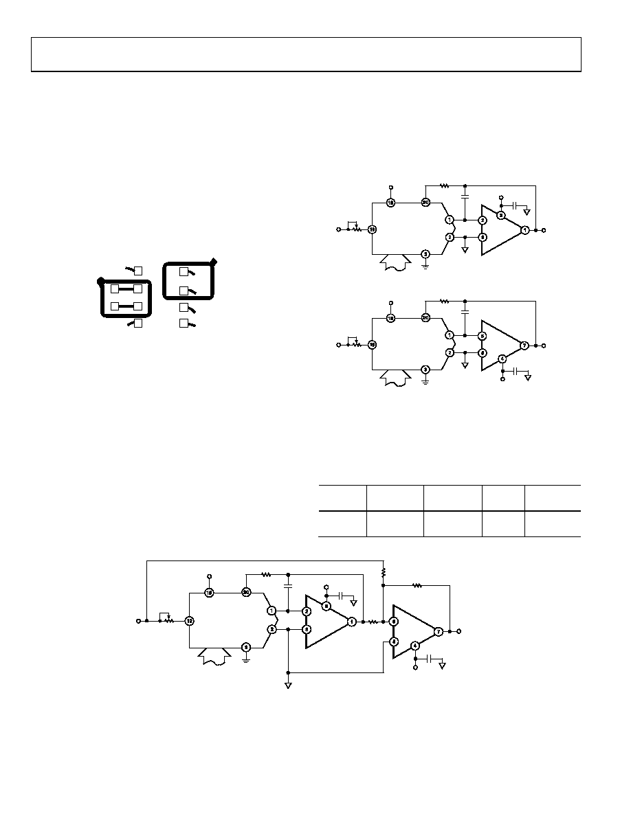
DAC CONVERTER APPLICATIONS
The AD712 is an excellent output amplifier for CMOS DACs. It can
be used to perform both 2-quadrant and 4-quadrant operations.
The output impedance of a DAC using an inverted R-2R ladder
approaches R for codes containing many 1s, and 3R for codes
containing a single 1. For codes containing all 0s, the output
impedance is infinite.
For example, the output resistance of the AD7545 modulates
between 11 kΩ and 33 kΩ. Therefore, with an 11 kΩ DAC
internal feedback resistance, the noise gain varies from 2 to 4/3.
This changing noise gain modulates the effect of the input offset
voltage of the amplifier, resulting in nonlinear DAC amplifier
performance.
The AD712K with guaranteed 700 μV offset voltage minimizes
this effect to achieve 12-bit performance.
CMOS DAC) configured for unipolar binary (2-quadrant multi-
plication) or bipolar (4-quadrant multiplication) operation.
Capacitor C1 provides phase compensation to reduce overshoot
and ringing.
+15V
1/2
AD712
VIN
VREF
VDD
RFB
OUT1
AGND
AD7545
DGND
VOUTA
R2A*
DB11 TO DB0
0.1F
VDD
R1A*
1/2
AD712
VIN
VREF
VDD
RFB
OUT1
AGND
AD7545
DGND
VOUTB
R2B*
DB11 TO DB0
0.1F
–15V
R1B*
VDD
C1A
33pF
ANALOG
COMMON
*REFER TO
TABLE 3
GAIN
ADJUST
C1B
33pF
ANALOG
COMMON
GAIN
ADJUST
*REFER TO
TABLE 3
+
–
+
–
008
23-
039
Figure 39. Unipolar Binary Operation
R1 and R2 calibrate the zero offset and gain error of the DAC.
Specific values for these resistors depend upon the grade of
AD7545 and are listed in Table 3.
Table 3. Recommended Trim Resistor Values vs. Grades of
Trim
Resistor
JN/AQ
KN/BQ
LN
GLN
R1
500 Ω
200 Ω
100 Ω
20 Ω
R2
150 Ω
68 Ω
33 Ω
6.8 Ω
+15V
1/2
AD712
VIN
VREF
RFB
OUT1
AGND
AD7545
DGND
R2*
DATA INPUT
0.1F
VDD
R1*
1/2
AD712
VOUT
0.1F
–15V
12
DB11 TO DB0
R4
20k
1%
R5
20k
1%
R3
10k
1%
C1
33pF
ANALOG
COMMON
VDD
GAIN
ADJUST
*FOR VALUES OF
R1 AND R2 SEE TABLE 3
+
–
+
–
00
82
3-
04
0
Figure 40. Bipolar Operation
相关PDF资料 |
PDF描述 |
|---|---|
| 0314012.MXP | FUSE CERAMIC 250V FAST 3AB 12A |
| LT1993IUD-10#PBF | IC DIFF AMP/ADC DRVR 16-QFN |
| SL1021B300RF | GAS TUBE 300V HVY 10KA 3PIN RADL |
| SL1021B260RF | GAS TUBE 260V HVY 10KA 3PIN RADL |
| SL1021B250RF | GAS TUBE 250V HVY 10KA 3PIN RADL |
相关代理商/技术参数 |
参数描述 |
|---|---|
| AD712KRZ-REEL7 | 功能描述:IC OPAMP BIFET DUAL PREC 8SOIC RoHS:是 类别:集成电路 (IC) >> Linear - Amplifiers - Instrumentation 系列:- 标准包装:73 系列:Over-The-Top® 放大器类型:通用 电路数:4 输出类型:满摆幅 转换速率:0.07 V/µs 增益带宽积:200kHz -3db带宽:- 电流 - 输入偏压:1nA 电压 - 输入偏移:285µV 电流 - 电源:50µA 电流 - 输出 / 通道:25mA 电压 - 电源,单路/双路(±):2 V ~ 44 V,±1 V ~ 22 V 工作温度:-40°C ~ 85°C 安装类型:表面贴装 封装/外壳:16-WFDFN 裸露焊盘 供应商设备封装:16-DFN-EP(5x3) 包装:管件 |
| AD712SCHIPS | 制造商:AD 制造商全称:Analog Devices 功能描述:Dual Precision, Low Cost, High Speed, BiFET Op Amp |
| AD712SH | 制造商:未知厂家 制造商全称:未知厂家 功能描述:Operational Amplifier |
| AD712SH/883B | 制造商:Analog Devices 功能描述:- Rail/Tube 制造商:Rochester Electronics LLC 功能描述: |
| AD712SQ | 制造商:AD 制造商全称:Analog Devices 功能描述:Dual Precision, Low Cost, High Speed, BiFET Op Amp |
发布紧急采购,3分钟左右您将得到回复。