- 您现在的位置:买卖IC网 > PDF目录8680 > AD7224KRZ-18REEL (Analog Devices Inc)IC DAC 8BIT W/OUTPUT AMPS 18SOIC PDF资料下载
参数资料
| 型号: | AD7224KRZ-18REEL |
| 厂商: | Analog Devices Inc |
| 文件页数: | 5/8页 |
| 文件大小: | 0K |
| 描述: | IC DAC 8BIT W/OUTPUT AMPS 18SOIC |
| 产品培训模块: | Data Converter Fundamentals DAC Architectures |
| 标准包装: | 1,000 |
| 设置时间: | 7µs |
| 位数: | 8 |
| 数据接口: | 并联 |
| 转换器数目: | 1 |
| 电压电源: | 双 ± |
| 功率耗散(最大): | 75mW |
| 工作温度: | -40°C ~ 85°C |
| 安装类型: | 表面贴装 |
| 封装/外壳: | 18-SOIC(0.295",7.50mm 宽) |
| 供应商设备封装: | 18-SOIC |
| 包装: | 带卷 (TR) |
| 输出数目和类型: | 1 电压,单极;1 电压,双极 |
| 采样率(每秒): | 143k |
AD7224
REV. B
–5–
VOUT = D VREF
where D is a fractional representation of the digital input code
and can vary from 0 to 255/256.
OP-AMP SECTION
The voltage-mode D/A converter output is buffered by a unity
gain noninverting CMOS amplifier. This buffer amplifier is
capable of developing +10 V across a 2 k
load and can drive
capacitive loads of 3300 pF.
The AD7224 can be operated single or dual supply resulting in
different performance in some parameters from the output am-
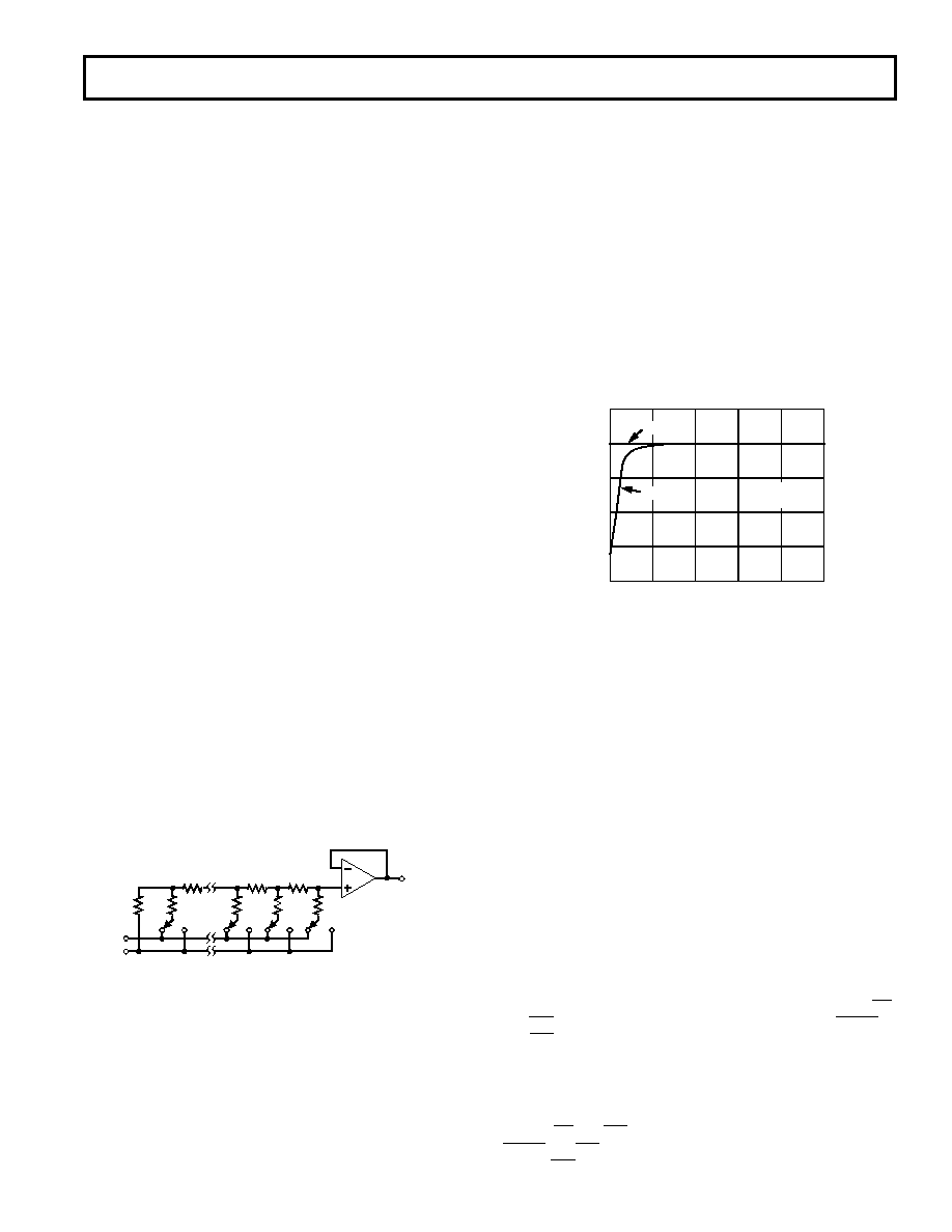
plifier. In single supply operation (VSS = 0 V = AGND) the sink
capability of the amplifier, which is normally 400
A, is reduced
as the output voltage nears AGND. The full sink capability of
400
A is maintained over the full output voltage range by tying
VSS to –5 V. This is indicated in Figure 2.
500
0
10
300
100
2
200
0
400
8
6
4
V
OUT – Volts
I SINK
–
A
V
SS = –5V
V
SS = 0V
V
DD = +15V
T
A = 25°C
Figure 2. Variation of ISINK with VOUT
Settling-time for negative-going output signals approaching
AGND is similarly affected by VSS. Negative-going settling-time
for single supply operation is longer than for dual supply opera-
tion. Positive-going settling-time is not affected by VSS.
Additionally, the negative VSS gives more headroom to the out-
put amplifier which results in better zero code performance and
improved slew-rate at the output, than can be obtained in the
single supply mode.
DIGITAL SECTION
The AD7224 digital inputs are compatible with either TTL or
5 V CMOS levels. All logic inputs are static-protected MOS
gates with typical input currents of less than 1 nA. Internal in-
put protection is achieved by an on-chip distributed diode be-
tween DGND and each MOS gate. To minimize power supply
currents, it is recommended that the digital input voltages be
driven as close to the supply rails (VDD and DGND) as practi-
cally possible.
INTERFACE LOGIC INFORMATION
Table I shows the truth table for AD7224 operation. The part
contains two registers, an input register and a DAC register. CS
and WR control the loading of the input register while LDAC
and WR control the transfer of information from the input regis-
ter to the DAC register. Only the data held in the DAC register
will determine the analog output of the converter.
All control signals are level-triggered and therefore either or
both registers may be made transparent; the input register by
keeping CS and WR “LOW”, the DAC register by keeping
LDAC
and WR “LOW”. Input data is latched on the rising
edge of WR.
TERMINOLOGY
TOTAL UNADJUSTED ERROR
Total Unadjusted Error is a comprehensive specification which
includes full-scale error, relative accuracy and zero code error.
Maximum output voltage is VREF – 1 LSB (ideal), where 1 LSB
(ideal) is VREF/256. The LSB size will vary over the VREF range.
Hence the zero code error, relative to the LSB size, will increase
as VREF decreases. Accordingly, the total unadjusted error,
which includes the zero code error, will also vary in terms of
LSBs over the VREF range. As a result, total unadjusted error is
specified for a fixed reference voltage of +10 V.
RELATIVE ACCURACY
Relative Accuracy or endpoint nonlinearity is a measure of the
maximum deviation from a straight line passing through the
endpoints of the DAC transfer function. It is measured after al-
lowing for zero code error and full-scale error and is normally
expressed in LSBs or as a percentage of full-scale reading.
DIFFERENTIAL NONLINEARITY
Differential Nonlinearity is the difference between the measured
change and the ideal 1 LSB change between any two adjacent
codes. A specified differential nonlinearity of
±1 LSB max over
the operating temperature range ensures monotonicity.
DIGITAL FEEDTHROUGH
Digital Feedthrough is the glitch impulse transferred to the out-
put due to a change in the digital input code. It is specified in
nV secs and is measured at VREF = 0 V.
FULL-SCALE ERROR
Full-Scale Error is defined as:
Measured Value – Zero Code Error – Ideal Value
CIRCUIT INFORMATION
D/A SECTION
The AD7224 contains an 8-bit voltage-mode digital-to-analog
converter. The output voltage from the converter has the same
polarity as the reference voltage, allowing single supply opera-
tion. A novel DAC switch pair arrangement on the AD7224 al-
lows a reference voltage range from +2 V to +12.5 V.
The DAC consists of a highly stable, thin-film, R-2R ladder and
eight high speed NMOS single pole, double-throw switches.
The simplified circuit diagram for this DAC is shown in
Figure 1.
V
OUT
RR
R
2R
DB0
V
REF
AGND
SHOWN FOR ALL 1's ON DAC
Figure 1. D/A Simplified Circuit Diagram
The input impedance at the VREF pin is code dependent and can
vary from 8 k
minimum to infinity. The lowest input imped-
ance occurs when the DAC is loaded with the digital code
01010101. Therefore, it is important that the reference presents
a low output impedance under changing load conditions. The
nodal capacitance at the reference terminals is also code depen-
dent and typically varies from 25 pF to 50 pF.
The VOUT pin can be considered as a digitally programmable
voltage source with an output voltage of:
相关PDF资料 |
PDF描述 |
|---|---|
| LTC1450CN#PBF | IC D/A CONV 12BIT R-R PAR 24-DIP |
| LTC1450CN | IC D/A CONV 12BIT R-R PAR 24-DIP |
| MC100H643FNG | IC CLK BUFFER 1:8 80MHZ 28-PLCC |
| MC10H645FNG | IC CLOCK BUFFER MUX 2:9 28-PLCC |
| VI-J12-MX-B1 | CONVERTER MOD DC/DC 15V 75W |
相关代理商/技术参数 |
参数描述 |
|---|---|
| AD7224KRZ-1REEL | 功能描述:IC DAC 8BIT W/AMP 20-SOIC RoHS:是 类别:集成电路 (IC) >> 数据采集 - 数模转换器 系列:- 标准包装:47 系列:- 设置时间:2µs 位数:14 数据接口:并联 转换器数目:1 电压电源:单电源 功率耗散(最大):55µW 工作温度:-40°C ~ 85°C 安装类型:表面贴装 封装/外壳:28-SSOP(0.209",5.30mm 宽) 供应商设备封装:28-SSOP 包装:管件 输出数目和类型:1 电流,单极;1 电流,双极 采样率(每秒):* |
| AD7224LCWN | 制造商:未知厂家 制造商全称:未知厂家 功能描述:8-Bit Digital-to-Analog Converter |
| AD7224LN | 功能描述:IC DAC 8BIT LC2MOS W/AMP 18-DIP RoHS:否 类别:集成电路 (IC) >> 数据采集 - 数模转换器 系列:- 产品培训模块:Data Converter Fundamentals DAC Architectures 标准包装:750 系列:- 设置时间:7µs 位数:16 数据接口:并联 转换器数目:1 电压电源:双 ± 功率耗散(最大):100mW 工作温度:0°C ~ 70°C 安装类型:表面贴装 封装/外壳:28-LCC(J 形引线) 供应商设备封装:28-PLCC(11.51x11.51) 包装:带卷 (TR) 输出数目和类型:1 电压,单极;1 电压,双极 采样率(每秒):143k |
| AD7224LNZ | 功能描述:IC DAC 8BIT LC2MOS W/AMP 18-DIP RoHS:是 类别:集成电路 (IC) >> 数据采集 - 数模转换器 系列:- 产品培训模块:Data Converter Fundamentals DAC Architectures 标准包装:750 系列:- 设置时间:7µs 位数:16 数据接口:并联 转换器数目:1 电压电源:双 ± 功率耗散(最大):100mW 工作温度:0°C ~ 70°C 安装类型:表面贴装 封装/外壳:28-LCC(J 形引线) 供应商设备封装:28-PLCC(11.51x11.51) 包装:带卷 (TR) 输出数目和类型:1 电压,单极;1 电压,双极 采样率(每秒):143k |
| AD7224LP | 功能描述:IC DAC 8BIT LC2MOS W/AMP 20PLCC RoHS:否 类别:集成电路 (IC) >> 数据采集 - 数模转换器 系列:- 产品培训模块:Data Converter Fundamentals DAC Architectures 标准包装:750 系列:- 设置时间:7µs 位数:16 数据接口:并联 转换器数目:1 电压电源:双 ± 功率耗散(最大):100mW 工作温度:0°C ~ 70°C 安装类型:表面贴装 封装/外壳:28-LCC(J 形引线) 供应商设备封装:28-PLCC(11.51x11.51) 包装:带卷 (TR) 输出数目和类型:1 电压,单极;1 电压,双极 采样率(每秒):143k |
发布紧急采购,3分钟左右您将得到回复。