参数资料
| 型号: | AD7225BQ |
| 厂商: | Analog Devices Inc |
| 文件页数: | 24/24页 |
| 文件大小: | 0K |
| 描述: | IC DAC 8BIT QUAD W/AMP 24-CDIP |
| 产品培训模块: | Data Converter Fundamentals DAC Architectures |
| 标准包装: | 15 |
| 设置时间: | 4µs |
| 位数: | 8 |
| 转换器数目: | 4 |
| 电压电源: | 双 ± |
| 功率耗散(最大): | 500mW |
| 工作温度: | -40°C ~ 85°C |
| 安装类型: | 通孔 |
| 封装/外壳: | 24-CDIP(0.300",7.62mm) |
| 供应商设备封装: | 24-CDIP |
| 包装: | 管件 |
| 输出数目和类型: | 4 电压,单极;4 电压,双极 |
| 采样率(每秒): | 200k |
AD7225
Rev. C | Page 9 of 24
CIRCUIT INFORMATION
DIGITAL-TO-ANALOG SECTION
The AD7225 contains four identical, 8-bit voltage mode digital-
to-analog converters. Each DAC has a separate reference input.
The output voltages from the converters have the same polarity
as the reference voltages, allowing single-supply operation. A novel
DAC switch pair arrangement on the AD7225 allows a refer-
ence voltage range from 2 V to 12.5 V on each reference input.
Each DAC consists of a highly stable, thin-film, R-2R ladder and
eight high speed NMOS, single-pole, double-throw switches. The
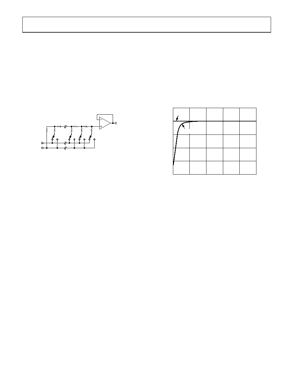
simplified circuit diagram for Channel A is shown in Figure 10.
Note that AGND is common to all four DACs.
VOUTA
2R
DB7
2R
DB6
2R
DB5
2R
DB0
R
VREFA
AGND
SHOWN FOR ALL 1s ON DAC
00986-
010
Figure 10. Digital-to-Analog Simplified Circuit Diagram
The input impedance at any of the reference inputs is code
dependent and can vary from 11 kΩ minimum to infinity. The
lowest input impedance at any reference input occurs when that
DAC is loaded with Digital Code 01010101. Therefore, it is
important that the reference presents a low output impedance
under changing load conditions. The nodal capacitance at the
reference terminals is also code dependent and typically varies
from 15 pF to 35 pF.
Each VOUTx pin can be considered a digitally programmable
voltage source with an output voltage of
VOUTX = DX × VREFX
where DX is a fractional representation of the digital input code
and can vary from 0 to 255/256.
The output impedance is that of the output buffer amplifier.
OP AMP SECTION
Each voltage mode DAC output is buffered by a unity gain
noninverting CMOS amplifier. This buffer amplifier is capable
of developing 10 V across a 2 kΩ load and can drive capacitive
loads of 3300 pF.
The AD7225 can be operated single or dual supply; operating
with dual supplies results in enhanced performance in some
parameters that cannot be achieved with single-supply opera-
tion. In single-supply operation (VSS = 0 V = AGND), the sink
capability of the amplifier, which is normally 400 μA, is reduced
as the output voltage nears AGND. The full sink capability of
400 μA is maintained over the full output voltage range by tying
Settling time for negative-going output signals approaching
AGND is similarly affected by VSS. Negative-going settling time
for single-supply operation is longer than for dual-supply opera-
tion. Positive-going settling time is not affected by VSS.
500
400
300
200
100
0
10
8
6
4
2
I S
INK
(
A)
VOUT (V)
VSS = –5V
VSS = 0V
VDD = +15V
TA = 25°C
00986-
011
Figure 11. Variation of ISINK with VOUT
Additionally, the negative VSS gives more headroom to the
output amplifiers, which results in better zero code perfor-
mance and improved slew rate at the output than can be
obtained in the single-supply mode.
DIGITAL INPUTS SECTION
The AD7225 digital inputs are compatible with either TTL or
5 V CMOS levels. All logic inputs are static protected MOS
gates with typical input currents of less than 1 nA. Internal
input protection is achieved by an on-chip distributed diode
between DGND and each MOS gate. To minimize power supply
currents, it is recommended that the digital input voltages be
driven as close to the supply rails (VDD and DGND) as practi-
cally possible.
相关PDF资料 |
PDF描述 |
|---|---|
| AD7226BQ | IC DAC 8BIT QUAD W/AMP 20-CDIP |
| AD7228CQ | IC DAC 8BIT OCTAL W/AMP 24-CDIP |
| AD7233BNZ | IC DAC 12BIT SRL W/AMP 8PDIP |
| AD7243BQ | IC DAC 12BIT W/AMP W/REF 16-CDIP |
| AD7244AQ | IC DAC 14BIT SRL W/REF 24-CDIP |
相关代理商/技术参数 |
参数描述 |
|---|---|
| AD7225BRS | 功能描述:IC DAC 8BIT QUAD W/AMP 24-SSOP RoHS:否 类别:集成电路 (IC) >> 数据采集 - 数模转换器 系列:- 标准包装:2,400 系列:- 设置时间:- 位数:18 数据接口:串行 转换器数目:3 电压电源:模拟和数字 功率耗散(最大):- 工作温度:-40°C ~ 85°C 安装类型:表面贴装 封装/外壳:36-TFBGA 供应商设备封装:36-TFBGA 包装:带卷 (TR) 输出数目和类型:* 采样率(每秒):* |
| AD7225BRS-REEL | 功能描述:IC DAC 8BIT QUAD W/AMP 24-SSOP RoHS:否 类别:集成电路 (IC) >> 数据采集 - 数模转换器 系列:- 产品培训模块:LTC263x 12-, 10-, and 8-Bit VOUT DAC Family 特色产品:LTC2636 - Octal 12-/10-/8-Bit SPI VOUT DACs with 10ppm/°C Reference 标准包装:91 系列:- 设置时间:4µs 位数:10 数据接口:MICROWIRE?,串行,SPI? 转换器数目:8 电压电源:单电源 功率耗散(最大):2.7mW 工作温度:-40°C ~ 85°C 安装类型:表面贴装 封装/外壳:14-WFDFN 裸露焊盘 供应商设备封装:14-DFN-EP(4x3) 包装:管件 输出数目和类型:8 电压,单极 采样率(每秒):* |
| AD7225BRSZ | 功能描述:IC DAC 8BIT QUAD W/AMP 24SSOP RoHS:是 类别:集成电路 (IC) >> 数据采集 - 数模转换器 系列:- 标准包装:47 系列:- 设置时间:2µs 位数:14 数据接口:并联 转换器数目:1 电压电源:单电源 功率耗散(最大):55µW 工作温度:-40°C ~ 85°C 安装类型:表面贴装 封装/外壳:28-SSOP(0.209",5.30mm 宽) 供应商设备封装:28-SSOP 包装:管件 输出数目和类型:1 电流,单极;1 电流,双极 采样率(每秒):* |
| AD7225CQ | 制造商:Rochester Electronics LLC 功能描述:CMOS DAC IC - Bulk |
| AD7225CRS | 功能描述:IC DAC 8BIT QUAD W/AMP 24-SSOP RoHS:否 类别:集成电路 (IC) >> 数据采集 - 数模转换器 系列:- 标准包装:47 系列:- 设置时间:2µs 位数:14 数据接口:并联 转换器数目:1 电压电源:单电源 功率耗散(最大):55µW 工作温度:-40°C ~ 85°C 安装类型:表面贴装 封装/外壳:28-SSOP(0.209",5.30mm 宽) 供应商设备封装:28-SSOP 包装:管件 输出数目和类型:1 电流,单极;1 电流,双极 采样率(每秒):* |
发布紧急采购,3分钟左右您将得到回复。