- 您现在的位置:买卖IC网 > PDF目录10801 > AD7225BRS (Analog Devices Inc)IC DAC 8BIT QUAD W/AMP 24-SSOP PDF资料下载
参数资料
| 型号: | AD7225BRS |
| 厂商: | Analog Devices Inc |
| 文件页数: | 1/24页 |
| 文件大小: | 0K |
| 描述: | IC DAC 8BIT QUAD W/AMP 24-SSOP |
| 产品培训模块: | Data Converter Fundamentals DAC Architectures |
| 产品变化通告: | Product Discontinuance 27/Oct/2011 |
| 标准包装: | 59 |
| 设置时间: | 4µs |
| 位数: | 8 |
| 转换器数目: | 4 |
| 电压电源: | 双 ± |
| 功率耗散(最大): | 500mW |
| 工作温度: | -40°C ~ 85°C |
| 安装类型: | 表面贴装 |
| 封装/外壳: | 24-SSOP(0.209",5.30mm 宽) |
| 供应商设备封装: | 24-SSOP |
| 包装: | 管件 |
| 输出数目和类型: | 4 电压,单极;4 电压,双极 |
| 采样率(每秒): | 200k |
LC2MOS Quad 8-Bit DAC
with Separate Reference Inputs
AD7225
Rev. C
Information furnished by Analog Devices is believed to be accurate and reliable. However, no
responsibilityis assumedbyAnalogDevicesforitsuse,norforanyinfringementsof patentsorother
rightsofthirdpartiesthatmayresultfromitsuse.Specificationssubjecttochangewithoutnotice.No
license is granted by implication or otherwise under any patent or patent rights of Analog Devices.
Trademarksandregisteredtrademarksarethepropertyoftheirrespectiveowners.
One Technology Way, P.O. Box 9106, Norwood, MA 02062-9106, U.S.A.
Tel: 781.329.4700
Fax: 781.461.3113
2010 Analog Devices, Inc. All rights reserved.
FEATURES
Four 8-bit DACs with output amplifiers
Separate reference input for each DAC
Microprocessor compatible with double-buffered inputs
Simultaneous update of all 4 outputs
Operates with single or dual supplies
Extended temperature range operation
No user trims required
Skinny 24-lead PDIP, CERDIP, SOIC, and SSOP packages
28-lead PLCC package
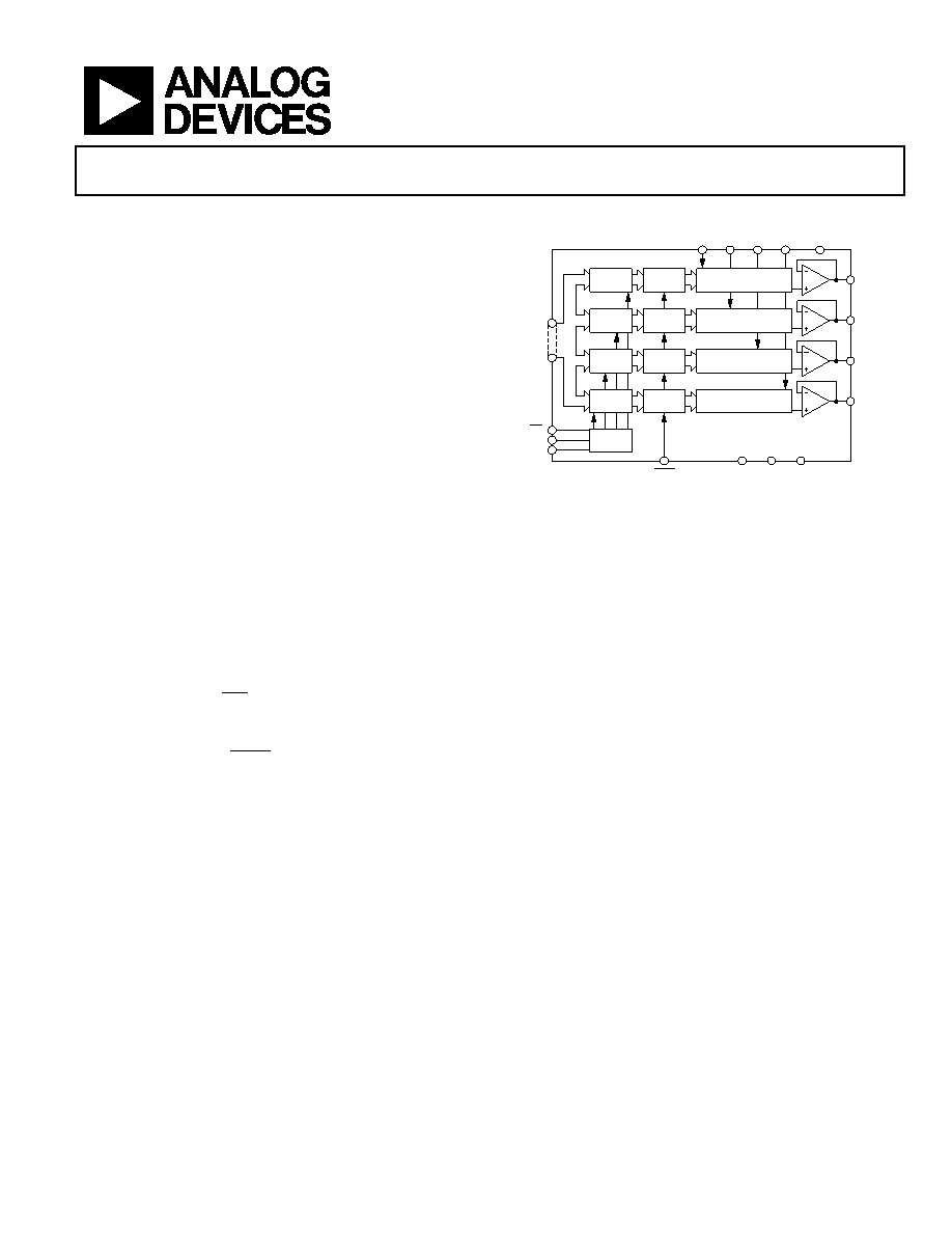
FUNCTIONAL BLOCK DIAGRAM
VREFA VREFB VREFC VREFD
VDD
LDAC
VSS
AGND DGND
INPUT
LATCH A
DAC
LATCH A
VOUTA
DAC A
A
INPUT
LATCH B
DAC
LATCH B
VOUTB
DAC B
B
INPUT
LATCH C
DAC
LATCH C
VOUTC
DAC C
C
INPUT
LATCH D
CONTROL
LOGIC
DAC
LATCH D
VOUTD
DAC D
D
DAT
A
BUS
DB7
DATA
(8-BIT)
DB0
WR
A1
A2
AD7225
00
986-
001
Figure 1.
GENERAL DESCRIPTION
The AD7225 contains four 8-bit voltage output digital-to-
analog converters, with output buffer amplifiers and interface
logic on a single monolithic chip. Each DAC has a separate
reference input terminal. No external trims are required to
achieve full specified performance for the part.
The double-buffered interface logic consists of two 8-bit
registers per channel—an input register and a DAC register.
Control Input A0 and Control Input A1 determine which input
register is loaded when WR goes low. Only the data held in the
DAC registers determines the analog outputs of the converters.
The double-buffering allows simultaneous update of all four
outputs under control of LDAC. All logic inputs are TTL and
CMOS (5 V) level compatible, and the control logic is speed
compatible with most 8-bit microprocessors.
Specified performance is guaranteed for input reference
voltages from 2 V to 12.5 V when using dual supplies. The part
is also specified for single-supply operation using a reference of
10 V. Each output buffer amplifier is capable of developing 10 V
across a 2 kΩ load.
The AD7225 is fabricated on an all ion-implanted, high speed,
linear-compatible CMOS (LC2MOS) process, which is
specifically developed to integrate high speed digital logic
circuits and precision analog circuitry on the same chip.
PRODUCT HIGHLIGHTS
1.
DACs and Amplifiers on CMOS Chip.
The single-chip design of four 8-bit DACs and amplifiers
allows a dramatic reduction in board space requirements
and offers increased reliability in systems using multiple
converters. Its pinout is aimed at optimizing board layout
with all analog inputs and outputs at one end of the
package and all digital inputs at the other.
2.
Single- or Dual-Supply Operation.
The voltage-mode configuration of the AD7225 allows
single-supply operation. The part can also be operated with
dual supplies, giving enhanced performance for some
parameters.
3.
Versatile Interface Logic.
The AD7225 has a common 8-bit data bus with individual
DAC latches, providing a versatile control architecture for
simple interface to microprocessors. The double-buffered
interface allows simultaneous update of the four outputs.
4.
Separate Reference Input for Each DAC.
The AD7225 offers great flexibility in dealing with input
signals, with a separate reference input provided for each
DAC and each reference having variable input voltage
capability.
相关PDF资料 |
PDF描述 |
|---|---|
| VE-JNJ-MW-F3 | CONVERTER MOD DC/DC 36V 100W |
| 85106P106PW50 | CONN PLUG STRAIGHT 6POS W/PIN |
| VE-JNJ-MW-F1 | CONVERTER MOD DC/DC 36V 100W |
| AD7224LR-18REEL | IC DAC 8BIT LC2MOS W/AMP 18SOIC |
| VE-JN4-MW-F4 | CONVERTER MOD DC/DC 48V 100W |
相关代理商/技术参数 |
参数描述 |
|---|---|
| AD7225BRS-REEL | 功能描述:IC DAC 8BIT QUAD W/AMP 24-SSOP RoHS:否 类别:集成电路 (IC) >> 数据采集 - 数模转换器 系列:- 产品培训模块:LTC263x 12-, 10-, and 8-Bit VOUT DAC Family 特色产品:LTC2636 - Octal 12-/10-/8-Bit SPI VOUT DACs with 10ppm/°C Reference 标准包装:91 系列:- 设置时间:4µs 位数:10 数据接口:MICROWIRE?,串行,SPI? 转换器数目:8 电压电源:单电源 功率耗散(最大):2.7mW 工作温度:-40°C ~ 85°C 安装类型:表面贴装 封装/外壳:14-WFDFN 裸露焊盘 供应商设备封装:14-DFN-EP(4x3) 包装:管件 输出数目和类型:8 电压,单极 采样率(每秒):* |
| AD7225BRSZ | 功能描述:IC DAC 8BIT QUAD W/AMP 24SSOP RoHS:是 类别:集成电路 (IC) >> 数据采集 - 数模转换器 系列:- 标准包装:47 系列:- 设置时间:2µs 位数:14 数据接口:并联 转换器数目:1 电压电源:单电源 功率耗散(最大):55µW 工作温度:-40°C ~ 85°C 安装类型:表面贴装 封装/外壳:28-SSOP(0.209",5.30mm 宽) 供应商设备封装:28-SSOP 包装:管件 输出数目和类型:1 电流,单极;1 电流,双极 采样率(每秒):* |
| AD7225CQ | 制造商:Rochester Electronics LLC 功能描述:CMOS DAC IC - Bulk |
| AD7225CRS | 功能描述:IC DAC 8BIT QUAD W/AMP 24-SSOP RoHS:否 类别:集成电路 (IC) >> 数据采集 - 数模转换器 系列:- 标准包装:47 系列:- 设置时间:2µs 位数:14 数据接口:并联 转换器数目:1 电压电源:单电源 功率耗散(最大):55µW 工作温度:-40°C ~ 85°C 安装类型:表面贴装 封装/外壳:28-SSOP(0.209",5.30mm 宽) 供应商设备封装:28-SSOP 包装:管件 输出数目和类型:1 电流,单极;1 电流,双极 采样率(每秒):* |
| AD7225CRS-REEL | 功能描述:IC DAC 8BIT QUAD W/AMP 24-SSOP RoHS:否 类别:集成电路 (IC) >> 数据采集 - 数模转换器 系列:- 标准包装:47 系列:- 设置时间:2µs 位数:14 数据接口:并联 转换器数目:1 电压电源:单电源 功率耗散(最大):55µW 工作温度:-40°C ~ 85°C 安装类型:表面贴装 封装/外壳:28-SSOP(0.209",5.30mm 宽) 供应商设备封装:28-SSOP 包装:管件 输出数目和类型:1 电流,单极;1 电流,双极 采样率(每秒):* |
发布紧急采购,3分钟左右您将得到回复。