参数资料
| 型号: | AD7226BQ |
| 厂商: | Analog Devices Inc |
| 文件页数: | 15/16页 |
| 文件大小: | 0K |
| 描述: | IC DAC 8BIT QUAD W/AMP 20-CDIP |
| 产品培训模块: | Data Converter Fundamentals DAC Architectures |
| 标准包装: | 18 |
| 设置时间: | 4µs |
| 位数: | 8 |
| 数据接口: | 并联 |
| 转换器数目: | 4 |
| 电压电源: | 双 ± |
| 工作温度: | -40°C ~ 85°C |
| 安装类型: | 通孔 |
| 封装/外壳: | 20-CDIP(0.300",7.62mm) |
| 供应商设备封装: | 20-CDIP |
| 包装: | 管件 |
| 输出数目和类型: | 4 电压,单极;4 电压,双极 |
| 采样率(每秒): | 143k |
REV.
–8–
AD7226
SPECIFICATION RANGES
In order for the DACs to operate to their specifications, the
reference voltage must be at least 4 V below the VDD power
supply voltage. This voltage differential is required for correct
generation of bias voltages for the DAC switches.
The AD7226 is specified to operate over a VDD range from
+12 V
± 5% to +15 V ± 10% (i.e., from +11.4 V to +16.5 V)
with a VSS of –5 V
± 10%. Operation is also specified for a single
+15 V
± 5% VDD supply. Applying a VSS of –5 V results in
improved zero code error, improved output sink capability with
outputs near AGND and improved negative-going settling time.
Performance is specified over a wide range of reference voltages
from 2 V to (VDD – 4 V) with dual supplies. This allows a range
of standard reference generators to be used such as the AD780,
a 2.5 V band gap reference and the AD584, a precision 10 V
reference. Note that in order to achieve an output voltage range
of 0 V to 10 V a nominal 15 V
± 5% power supply voltage is
required by the AD7226.
SETTLING TIME
The output stage of the buffer amplifiers consists of a bipolar
NPN transistor from the VDD line and a constant current load to
VSS. VSS is the negative power supply for the output buffer ampli-
fiers. As mentioned in the op amp section, in single supply
operation the NMOS transistor will come out of saturation as the
output voltage approaches AGND and will act as a resistive load
of approximately 2 k
W to AGND. As a result, the settling time for
negative-going signals approaching AGND in single supply opera-
tion will be longer than for dual supply operation where the
current load of 400
mA is maintained all the way down to AGND.
Positive-going settling-time is not affected by VSS.
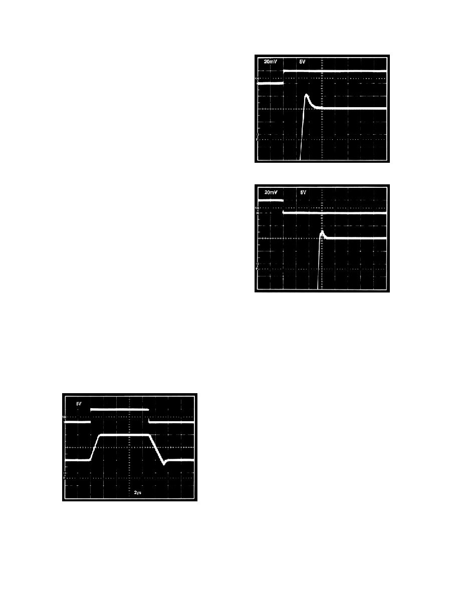
The settling-time for the AD7226 is limited by the slew-rate of
the output buffer amplifiers. This can be seen from Figure 6
which shows the dynamic response for the AD7226 for a full
scale change. Figures 7a and 7b show expanded settling-time
photographs with the output waveforms derived from a differen-
tial input to an oscilloscope. Figure 7a shows the settling time
for a positive-going step and Figure 7b shows the settling time
for a negative-going output step.
DATA
VOUT
Figure 6. Dynamic Response (VSS = –5 V)
DATA
O/P
+1/2 LSB
–1/2 LSB
Figure 7a. Positive Step Settling Time (VSS = –5 V)
DATA
O/P
+1/2 LSB
–1/2 LSB
Figure 7b. Negative Step Settling Time (VSS = –5 V)
GROUND MANAGEMENT
AC or transient voltages between AGND and DGND can cause
noise at the analog output. This is especially true in micropro-
cessor systems where digital noise is prevalent. The simplest
method of ensuring that voltages at AGND and DGND are
equal is to tie AGND and DGND together at the AD7226. In
more complex systems where the AGND and DGND intertie is
on the backplane, it is recommended that two diodes be con-
nected in inverse parallel between the AD7226 AGND and
DGND pins (IN914 or equivalent).
Unipolar Output Operation
This is the basic mode of operation for each channel of the
AD7226, with the output voltage having the same positive
polarity as +VREF. The AD7226 can be operated single supply
(VSS = AGND) or with positive/negative supplies (see op amp
section which outlines the advantages of having negative VSS).
The code table for unipolar output operation is shown in Table
II. Note that the voltage at VREF must never be negative with
respect to DGND in order to prevent parasitic transistor turn-on.
Connections for the unipolar output operation are shown in
Figure 8.
D
相关PDF资料 |
PDF描述 |
|---|---|
| AD7228CQ | IC DAC 8BIT OCTAL W/AMP 24-CDIP |
| AD7233BNZ | IC DAC 12BIT SRL W/AMP 8PDIP |
| AD7243BQ | IC DAC 12BIT W/AMP W/REF 16-CDIP |
| AD7244AQ | IC DAC 14BIT SRL W/REF 24-CDIP |
| AD7247AQ | IC DAC 12BIT W/AMP W/BUFF 24CDIP |
相关代理商/技术参数 |
参数描述 |
|---|---|
| AD7226BQ/+ | 制造商:未知厂家 制造商全称:未知厂家 功能描述:8-Bit Digital-to-Analog Converter |
| AD7226BRS | 制造商:Rochester Electronics LLC 功能描述:CMOS QUAD 8 BIT D/A CONVERTER V-OUT I.C. - Bulk 制造商:Analog Devices 功能描述: |
| AD7226BRS-REEL | 制造商:Analog Devices 功能描述:DAC 4-CH R-2R 8-bit 20-Pin SSOP T/R 制造商:Analog Devices 功能描述:DAC 4-CH R-2R 8BIT 20SSOP - Tape and Reel 制造商:Rochester Electronics LLC 功能描述:CMOS QUAD 8 BIT D/A CONVERTER V-OUT I.C. - Tape and Reel 制造商:Analog Devices 功能描述:Digital to Analog Converter |
| AD7226BRSZ | 功能描述:IC DAC 8BIT QUAD W/AMP 20SSOP RoHS:是 类别:集成电路 (IC) >> 数据采集 - 数模转换器 系列:- 标准包装:1 系列:- 设置时间:4.5µs 位数:12 数据接口:串行,SPI? 转换器数目:1 电压电源:单电源 功率耗散(最大):- 工作温度:-40°C ~ 125°C 安装类型:表面贴装 封装/外壳:8-SOIC(0.154",3.90mm 宽) 供应商设备封装:8-SOICN 包装:剪切带 (CT) 输出数目和类型:1 电压,单极;1 电压,双极 采样率(每秒):* 其它名称:MCP4921T-E/SNCTMCP4921T-E/SNRCTMCP4921T-E/SNRCT-ND |
| AD7226KC/D | 制造商:未知厂家 制造商全称:未知厂家 功能描述:8-Bit Digital-to-Analog Converter |
发布紧急采购,3分钟左右您将得到回复。