参数资料
| 型号: | AD7226KPZ |
| 厂商: | Analog Devices Inc |
| 文件页数: | 16/16页 |
| 文件大小: | 0K |
| 描述: | IC DAC 8BIT LC2MOS QUAD 20-PLCC |
| 产品培训模块: | Data Converter Fundamentals DAC Architectures |
| 标准包装: | 1 |
| 设置时间: | 4µs |
| 位数: | 8 |
| 数据接口: | 并联 |
| 转换器数目: | 4 |
| 电压电源: | 双 ± |
| 工作温度: | -40°C ~ 85°C |
| 安装类型: | 表面贴装 |
| 封装/外壳: | 20-LCC(J 形引线) |
| 供应商设备封装: | 20-PLCC(9x9) |
| 包装: | 管件 |
| 输出数目和类型: | 4 电压,单极;4 电压,双极 |
| 采样率(每秒): | 143k |
REV.
AD7226
–9–
DAC A
DAC B
DAC C
DAC D
MSB
VREF
VDD
DGND
AGND
VSS
VOUTA
WR
A1
A0
LSB
VOUTB
VOUTC
VOUTD
DB7
DB0
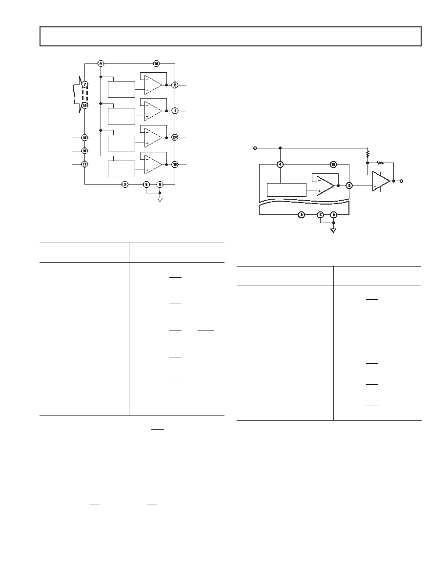
Figure 8. AD7226 Unipolar Output Circuit
Table II. Unipolar Code Table
DAC Latch Contents
MSB
LSB
Analog Output
1 1 1 1
+
VREF
255
256
1 0 0 0
0 0 0 1
+
VREF
129
256
1 0 0 0
0 0 0 0
+
=+
V
REF
128
256
2
0 1 1 1
1 1 1 1
+
VREF
127
256
0 0 0 0
0 0 0 1
+
VREF
1
256
0 0 0 0
0 V
Note LSB
V
REF
:
–
=
()
()=
2
1
256
8
(2)
Bipolar Output Operation
Each of the DACs of the AD7226 can be individually config-
ured to provide bipolar output operation. This is possible using
one external amplifier and two resistors per channel. Figure 9
shows a circuit used to implement offset binary coding (bipolar
operation) with DAC A of the AD7226. In this case
V
R
DV
R
V
OUT
A
REF
=+
()
()
1
2
1
2
1
–
(3)
With R1 = R2
VD
V
OUT
A
REF
=
()
21
–
(4)
where DA is a fractional representation of the digital word in latch A.
Mismatch between R1 and R2 causes gain and offset errors and
therefore these resistors must match and track over tempera-
ture. Once again the AD7226 can be operated in single supply
or from positive/negative supplies. Table III shows the digital
code versus output voltage relationship for the circuit of Figure 9
with R1 = R2.
DAC A
VREF
VDD
DGND
AGND
VSS
VOUTA
VOUT
VREF
AD7226*
R2
R1
+15V
–15V
R1, R2 = 10k
0.1%
*DIGITAL INPUTS OMITTED
FOR CLARITY
Figure 9. AD7226 Bipolar Output Circuit
Table III. Bipolar (Offset Binary) Code Table
DAC Latch Contents
MSB
LSB
Analog Output
1 1 1 1
+
VREF
127
128
1 0 0 0
0 0 0 1
+
VREF
1
128
1 0 0 0
0 0 0 0
0 V
0 1 1 1
1 1 1 1
–VREF
1
128
0 0 0 0
0 0 0 1
–VREF
127
128
0 0 0 0
––
VV
REF
128
=
AGND BIAS
The AD7226 AGND pin can be biased above system GND
(AD7226 DGND) to provide an offset “zero” analog output
voltage level. Figure 10 shows a circuit configuration to achieve
this for channel A of the AD7226. The output voltage, VOUTA,
can be expressed as:
VA
V
D V
OUT
BIAS
A
IN
=+
()
(5)
where DA is a fractional representation of the digital input word
(0
D 255/256).
D
相关PDF资料 |
PDF描述 |
|---|---|
| D38999/20SE6SA | CONN RCPT 6POS WALL MNT W/SCKT |
| AD7548BQ | IC DAC 12BIT MONO LC2MOS 20-CDIP |
| MS27473T16F8PLC | CONN HSG PLUG 8POS STRGHT PINS |
| AD7538KNZ | IC DAC 14BIT W/BUFFER 24DIP |
| VE-2WM-MY-F3 | CONVERTER MOD DC/DC 10V 50W |
相关代理商/技术参数 |
参数描述 |
|---|---|
| AD7226KPZ | 制造商:Analog Devices 功能描述:IC 8-BIT DAC |
| AD7226KPZ-REEL | 功能描述:IC DAC 8BIT QUAD W/AMP 20PLCC RoHS:是 类别:集成电路 (IC) >> 数据采集 - 数模转换器 系列:- 产品培训模块:Data Converter Fundamentals DAC Architectures 标准包装:750 系列:- 设置时间:7µs 位数:16 数据接口:并联 转换器数目:1 电压电源:双 ± 功率耗散(最大):100mW 工作温度:0°C ~ 70°C 安装类型:表面贴装 封装/外壳:28-LCC(J 形引线) 供应商设备封装:28-PLCC(11.51x11.51) 包装:带卷 (TR) 输出数目和类型:1 电压,单极;1 电压,双极 采样率(每秒):143k |
| AD7226KR | 功能描述:IC DAC 8BIT LC2MOS QUAD 20-SOIC RoHS:否 类别:集成电路 (IC) >> 数据采集 - 数模转换器 系列:- 产品培训模块:Data Converter Fundamentals DAC Architectures 标准包装:750 系列:- 设置时间:7µs 位数:16 数据接口:并联 转换器数目:1 电压电源:双 ± 功率耗散(最大):100mW 工作温度:0°C ~ 70°C 安装类型:表面贴装 封装/外壳:28-LCC(J 形引线) 供应商设备封装:28-PLCC(11.51x11.51) 包装:带卷 (TR) 输出数目和类型:1 电压,单极;1 电压,双极 采样率(每秒):143k |
| AD7226KR-REEL | 功能描述:IC DAC 8BIT QUAD W/AMP 20-SOIC RoHS:否 类别:集成电路 (IC) >> 数据采集 - 数模转换器 系列:- 产品培训模块:Data Converter Fundamentals DAC Architectures 标准包装:750 系列:- 设置时间:7µs 位数:16 数据接口:并联 转换器数目:1 电压电源:双 ± 功率耗散(最大):100mW 工作温度:0°C ~ 70°C 安装类型:表面贴装 封装/外壳:28-LCC(J 形引线) 供应商设备封装:28-PLCC(11.51x11.51) 包装:带卷 (TR) 输出数目和类型:1 电压,单极;1 电压,双极 采样率(每秒):143k |
| AD7226KRS | 制造商:Rochester Electronics LLC 功能描述:- Bulk |
发布紧急采购,3分钟左右您将得到回复。