参数资料
| 型号: | AD7228ACPZ |
| 厂商: | Analog Devices Inc |
| 文件页数: | 6/8页 |
| 文件大小: | 0K |
| 描述: | IC DAC 8BIT OCTAL W/AMP 28-PLCC |
| 产品培训模块: | Data Converter Fundamentals DAC Architectures |
| 标准包装: | 1 |
| 设置时间: | 5µs |
| 位数: | 8 |
| 数据接口: | 并联 |
| 转换器数目: | 8 |
| 电压电源: | 双 ± |
| 功率耗散(最大): | 310mW |
| 工作温度: | -40°C ~ 85°C |
| 安装类型: | 表面贴装 |
| 封装/外壳: | 28-LCC(J 形引线) |
| 供应商设备封装: | 28-PLCC(11.51x11.51) |
| 包装: | 管件 |
| 输出数目和类型: | 8 电压,单极;8 电压,双极 |
| 采样率(每秒): | 200k |
AD7228A
REV. A
–6–
Table II. Unipolar Code Table
DAC Latch Contents
MSB
LSB
Analog Output
1 1 1 1
+V
REF
255
256
1 0 0 0
0 0 0 1
+V
REF
129
256
1 0 0 0
0 0 0 0
+V
REF
128
256
=+
V
REF
2
0 1 1 1
1 1 1 1
+V
REF
127
256
0 0 0 0
0 0 0 1
+V
REF
1
256
0 0 0 0
0 V
Note: 1 LSB = (VREF)(2
–8) = V
REF
1
256
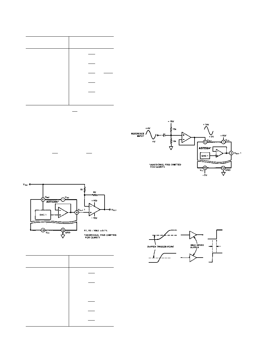
BIPOLAR OUTPUT OPERATION
Each of the DACs on the AD7228A can be individually config-
ured for bipolar output operation. This is possible using one ex-
ternal amplifier and two resistors per channel. Figure 8 shows a
circuit used to implement offset binary coding (bipolar opera-
tion) with DAC1 of the AD7228A. In this case
V
OUT =
1
+ R2
R1
D
1 V REF
() – R2
R1
V
REF
()
With R1 = R2
VOUT = (2D1 – 1) (VREF)
where D1 is a fractional representation of the digital word in
latch 1 of the AD7228A. (0
≤ D
1
≤ 255/256)
Figure 8. Bipolar Output Circuit
Table III. Bipolar Code Table
DAC Latch Contents
MSB
LSB
Analog Output
1 1 1 1
+V
REF
127
128
1 0 0 0
0 0 0 1
+V
REF
1
128
1 0 0 0
0 0 0 0
0 V
0 1 1 1
1 1 1 1
–V
REF
1
128
0 0 0 0
0 0 0 1
–V
REF
127
128
0 0 0 0
–V
REF
128
= –V
REF
Mismatch between R1 and R2 causes gain and offset errors, and
therefore, these resistors must match and track over temperature.
Once again, the AD7228A can be operated from single supply
or from dual supplies. Table III shows the digital code versus
output voltage relationship for the circuit of Figure 8 with
R1 = R2.
AC REFERENCE SIGNAL
In some applications it may be desirable to have an ac signal ap-
plied as the reference input to the AD7228A. The AD7228A
has multiplying capability within the upper (+10 V) and lower
(+2 V) limits of reference voltage when operated with dual sup-
plies. Therefore, ac signals need to be ac coupled and biased up
before being applied to the reference input. Figure 9 shows a
sine-wave signal applied to the reference input of the AD7228A.
For input frequencies up to 50 kHz, the output distortion typi-
cally remains less than 0.1%. The typical 3 dB bandwidth for
small signal inputs is 800 kHz.
Figure 9. Applying a AC Signal to the AD7228A
TIMING DESKEW
A common problem in ATE applications is the slowing or
“rounding-off” of signal edges by the time they reach the
pin-driver circuitry. This problem can easily be overcome by
“squaring-up” the edge at the pin-driver. However, since each
edge will not have been “rounded-off” by the same extent, this
“squaring-up” could lead to incorrect timing relationship be-
tween signals. This effect is shown in Figure 10a.
Figure 10a. Time Skewing Due to Slowing of Edges
The circuit of Figure 10b shows how two DACs of the
AD7228A can help in overcoming this problem. The same two
signals are applied to this circuit as were applied in Figure 10b.
The output of each DAC is applied to one input of a high-speed
comparator, and the signals are applied to the other inputs.
Varying the output voltage of the DAC effectively varies the
trigger point at which the comparator flips. Thus the timing re-
lationship between the two signals can be programmably cor-
rected (or deskewed) by varying the code to the DAC of the
AD7228A. In a typical application, the code is loaded to the
相关PDF资料 |
PDF描述 |
|---|---|
| VE-BWK-MY-F1 | CONVERTER MOD DC/DC 40V 50W |
| VE-BW1-MV-F4 | CONVERTER MOD DC/DC 12V 150W |
| AD5542CRZ | IC DAC 16BIT SERIAL-IN 14-SOIC |
| MS27505E13B4PLC | CONN HSG RCPT 4POS BOX MNT PINS |
| AD5762RCSUZ | IC DAC DUAL 16BIT 1LSB 32-TQFP |
相关代理商/技术参数 |
参数描述 |
|---|---|
| AD7228ACPZ-REEL | 功能描述:IC DAC 8BIT OCTAL W/AMP 28-PLCC RoHS:是 类别:集成电路 (IC) >> 数据采集 - 数模转换器 系列:- 产品培训模块:Data Converter Fundamentals DAC Architectures 标准包装:750 系列:- 设置时间:7µs 位数:16 数据接口:并联 转换器数目:1 电压电源:双 ± 功率耗散(最大):100mW 工作温度:0°C ~ 70°C 安装类型:表面贴装 封装/外壳:28-LCC(J 形引线) 供应商设备封装:28-PLCC(11.51x11.51) 包装:带卷 (TR) 输出数目和类型:1 电压,单极;1 电压,双极 采样率(每秒):143k |
| AD7228ACQ | 功能描述:IC DAC 8BIT OCTAL W/AMP 24-CDIP RoHS:否 类别:集成电路 (IC) >> 数据采集 - 数模转换器 系列:- 产品培训模块:Lead (SnPb) Finish for COTS Obsolescence Mitigation Program 标准包装:1,000 系列:- 设置时间:1µs 位数:8 数据接口:串行 转换器数目:8 电压电源:双 ± 功率耗散(最大):941mW 工作温度:0°C ~ 70°C 安装类型:表面贴装 封装/外壳:24-SOIC(0.295",7.50mm 宽) 供应商设备封装:24-SOIC W 包装:带卷 (TR) 输出数目和类型:8 电压,单极 采样率(每秒):* |
| AD7228ACR | 功能描述:IC DAC 8BIT LC2MOS OCTAL 24SOIC RoHS:否 类别:集成电路 (IC) >> 数据采集 - 数模转换器 系列:- 产品培训模块:Data Converter Fundamentals DAC Architectures 标准包装:750 系列:- 设置时间:7µs 位数:16 数据接口:并联 转换器数目:1 电压电源:双 ± 功率耗散(最大):100mW 工作温度:0°C ~ 70°C 安装类型:表面贴装 封装/外壳:28-LCC(J 形引线) 供应商设备封装:28-PLCC(11.51x11.51) 包装:带卷 (TR) 输出数目和类型:1 电压,单极;1 电压,双极 采样率(每秒):143k |
| AD7228ACR-REEL | 功能描述:IC DAC 8BIT OCTAL W/AMP 24-SOIC RoHS:否 类别:集成电路 (IC) >> 数据采集 - 数模转换器 系列:- 产品培训模块:Data Converter Fundamentals DAC Architectures 标准包装:750 系列:- 设置时间:7µs 位数:16 数据接口:并联 转换器数目:1 电压电源:双 ± 功率耗散(最大):100mW 工作温度:0°C ~ 70°C 安装类型:表面贴装 封装/外壳:28-LCC(J 形引线) 供应商设备封装:28-PLCC(11.51x11.51) 包装:带卷 (TR) 输出数目和类型:1 电压,单极;1 电压,双极 采样率(每秒):143k |
| AD7228ACRZ | 功能描述:IC DAC 8BIT LC2MOS OCTAL 24SOIC RoHS:是 类别:集成电路 (IC) >> 数据采集 - 数模转换器 系列:- 产品培训模块:Lead (SnPb) Finish for COTS Obsolescence Mitigation Program 标准包装:50 系列:- 设置时间:4µs 位数:12 数据接口:串行 转换器数目:2 电压电源:单电源 功率耗散(最大):- 工作温度:-40°C ~ 85°C 安装类型:表面贴装 封装/外壳:8-TSSOP,8-MSOP(0.118",3.00mm 宽) 供应商设备封装:8-uMAX 包装:管件 输出数目和类型:2 电压,单极 采样率(每秒):* 产品目录页面:1398 (CN2011-ZH PDF) |
发布紧急采购,3分钟左右您将得到回复。