参数资料
| 型号: | AD7233ANZ |
| 厂商: | Analog Devices Inc |
| 文件页数: | 7/8页 |
| 文件大小: | 0K |
| 描述: | IC DAC 12BIT LC2MOS SRL 8-DIP |
| 产品培训模块: | Data Converter Fundamentals DAC Architectures |
| 标准包装: | 50 |
| 系列: | DACPORT® |
| 设置时间: | 10µs |
| 位数: | 12 |
| 数据接口: | 串行 |
| 转换器数目: | 1 |
| 电压电源: | 双 ± |
| 功率耗散(最大): | 168mW |
| 工作温度: | -40°C ~ 85°C |
| 安装类型: | 通孔 |
| 封装/外壳: | 8-DIP(0.300",7.62mm) |
| 供应商设备封装: | 8-PDIP |
| 包装: | 管件 |
| 输出数目和类型: | 1 电压,双极 |
| 采样率(每秒): | 300k |
AD7233
REV. B
–7–
MICROPROCESSOR INTERFACING
Microprocessor interfacing to the AD7233 is via a serial bus that
uses standard protocol compatible with DSP processors and
microcontrollers. The communications channel requires a
three-wire interface consisting of a clock signal, a data signal, and
a synchronization signal. The AD7233 requires a 16-bit data
word with data valid on the falling edge of SCLK. For all of the
interfaces, the DAC update may be done automatically when all
the data is clocked in or it may done under control of
LDAC.
Figures 5 to 8 show the AD7233 configured for interfacing to a
number of popular DSP processors and microcontrollers.
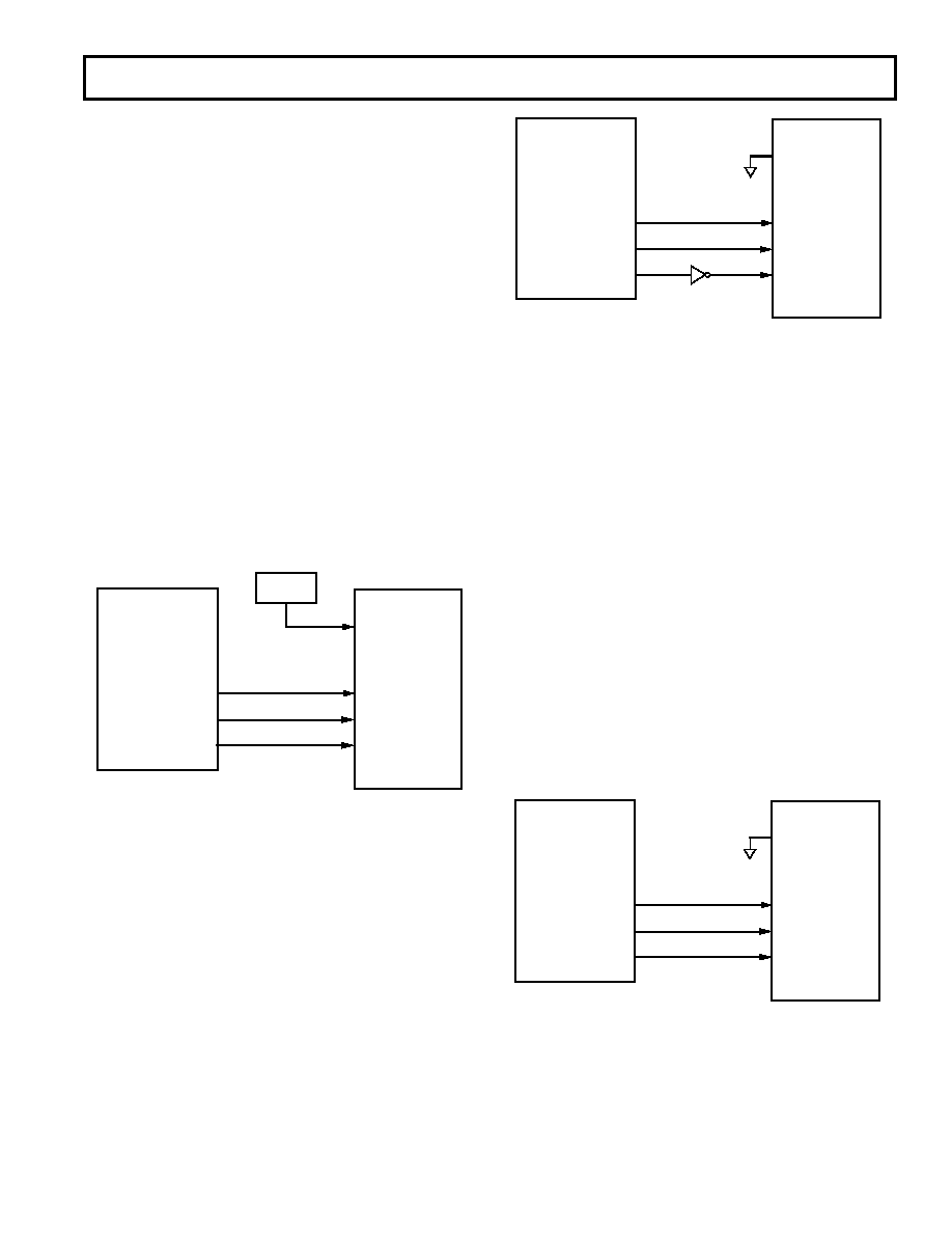
AD7233–ADSP-2101/ADSP-2102 Interface
Figure 5 shows a serial interface between the AD7233 and the
ADSP-2101/ADSP-2102 DSP processor. The ADSP-2101/
ADSP-2102 contains two serial ports, and either port may be
used in the interface. The data transfer is initiated by
TFS going
low. Data from the ADSP-2101/ADSP-2102 is clocked into the
AD7233 on the falling edge of SCLK. When the data transfer is
complete
TFS is taken high. In the interface shown the DAC is
updated using an external timer which generates an
LDAC pulse.
This could also be done using a control or decoded address line
from the processor. Alternatively, the
LDAC input could be
hardwired low, and in this case the automatic update mode is
selected whereby the DAC update takes place automatically on
the 16th falling edge of SCLK.
TIMER
ADSP-2102*
SCLK
DT
TFS
ADSP-2101/
LDAC
SYNC
SCLK
*ADDITIONAL PINS OMITTED FOR CLARITY
AD7233*
SDIN
Figure 5. AD7233 to ADSP-2101/ADSP-2102 Interface
AD7233-DSP56000 Interface
A serial interface between the AD7233 and the DSP56000 is
shown in Figure 6. The DSP56000 is configured for Normal Mode
Asynchronous operation with Gated Clock. It is also set up for a
16-bit word with SCK and SC2 as outputs and the FSL control bit
set to a 0. SCK is internally generated on the DSP56000 and
applied to the AD7233 SCLK input. Data from the DSP56000 is
valid on the falling edge of SCK. The SC2 output provides the
framing pulse for valid data. This line must be inverted before
being applied to the
SYNC input of the AD7233.
The
LDAC input of the AD7233 is connected to GND so the
update of the DAC latch takes place automatically on the 16th
falling edge of SCLK. An external timer could also be used as in
the previous interface if an external update is required.
DSP56000
SCK
STD
SC2
LDAC
SYNC
SCLK
*ADDITIONAL PINS OMITTED FOR CLARITY
AD7233*
SDIN
Figure 6. AD7233 to DSP56000 Interface
AD7233–87C51 Interface
A serial interface between the AD7233 and the 87C51 micro-
controller is shown in Figure 7. TXD of the 87C51 drives
SCLK of the AD7233 while RXD drives the serial data line of
the part. The
SYNC signal is derived from the port line P3.3.
The 87C51 provides the LSB of its SBUF register as the first bit
in the serial data stream. Therefore, the user will have to ensure
that the data in the SBUF register is arranged correctly so that
the don’t care bits are the first to be transmitted to the AD7233
and the last bit to be sent is the LSB of the word to be loaded to
the AD7233. When data is to be transmitted to the part, P3.3 is
taken low. Data on RXD is valid on the falling edge of TXD.
The 87C51 transmits its serial data in 8-bit bytes with only eight
falling clock edges occurring in the transmit cycle. To load data
to the AD7233, P3.3 is kept low after the first eight bits are
transferred and a second byte of data is then transferred serially
to the AD7233. When the second serial transfer is complete, the
P3.3 line is taken high.
Figure 7 shows the
LDAC input of the AD7233 hardwired low.
As a result, the DAC latch and the analog output will be updated
on the sixteenth falling edge of TXD after the
SYNC signal for
the DAC has gone low. Alternatively, the scheme used in previ-
ous interfaces, whereby the
LDAC input is driven from a timer,
can be used.
87C51*
P3.3
TXD
RXD
LDAC
SYNC
SCLK
*ADDITIONAL PINS OMITTED FOR CLARITY
AD7233*
SDIN
Figure 7. AD7233 to 87C51 Interface
相关PDF资料 |
PDF描述 |
|---|---|
| VE-BND-MV-F3 | CONVERTER MOD DC/DC 85V 150W |
| VE-BNH-MV-F4 | CONVERTER MOD DC/DC 52V 150W |
| VE-BNH-MV-F2 | CONVERTER MOD DC/DC 52V 150W |
| VE-BNH-MV-F1 | CONVERTER MOD DC/DC 52V 150W |
| JL05-2A24-52ASCW-F0-R | CONN RCPT 52POS CRIMP W/O SOCKET |
相关代理商/技术参数 |
参数描述 |
|---|---|
| AD7233ANZ | 制造商:Analog Devices 功能描述:D/A Converter (D-A) IC |
| AD7233BN | 制造商:Analog Devices 功能描述:DAC 1-CH R-2R 12-bit 8-Pin PDIP Tube 制造商:Analog Devices 功能描述:SEMICONDUCTORSLINEAR |
| AD7233BNZ | 功能描述:IC DAC 12BIT SRL W/AMP 8PDIP RoHS:是 类别:集成电路 (IC) >> 数据采集 - 数模转换器 系列:DACPORT® 产品培训模块:Lead (SnPb) Finish for COTS Obsolescence Mitigation Program 标准包装:50 系列:- 设置时间:4µs 位数:12 数据接口:串行 转换器数目:2 电压电源:单电源 功率耗散(最大):- 工作温度:-40°C ~ 85°C 安装类型:表面贴装 封装/外壳:8-TSSOP,8-MSOP(0.118",3.00mm 宽) 供应商设备封装:8-uMAX 包装:管件 输出数目和类型:2 电压,单极 采样率(每秒):* 产品目录页面:1398 (CN2011-ZH PDF) |
| AD7237 | 制造商:AD 制造商全称:Analog Devices 功能描述:LC2MOS DUAL 12-BIT DACPORT |
| AD7237A | 制造商:AD 制造商全称:Analog Devices 功能描述:LC2MOS Dual 12-Bit DACPORTs |
发布紧急采购,3分钟左右您将得到回复。