参数资料
| 型号: | AD7237AQ |
| 厂商: | Analog Devices Inc |
| 文件页数: | 11/12页 |
| 文件大小: | 0K |
| 描述: | IC DAC 12BIT W/AMP W/BUFF 24CDIP |
| 产品培训模块: | Data Converter Fundamentals DAC Architectures |
| 标准包装: | 15 |
| 系列: | DACPORT® |
| 设置时间: | 8µs |
| 位数: | 12 |
| 数据接口: | 并联 |
| 转换器数目: | 2 |
| 电压电源: | 双 ± |
| 工作温度: | -40°C ~ 85°C |
| 安装类型: | 通孔 |
| 封装/外壳: | 24-CDIP(0.300",7.62mm) |
| 供应商设备封装: | 24-CDIP |
| 包装: | 管件 |
| 输出数目和类型: | 2 电压,单极;2 电压,双极 |
| 采样率(每秒): | * |
AD7237A/AD7247A
REV. 0
–8–
CIRCUIT INFORMATION
D/A Section
The AD7237A/AD7247A contains two 12-bit voltage-mode D/A
converters consisting of highly stable thin film resistors and high
speed NMOS single-pole, double-throw switches. The output
voltage from the converters has the same polarity as the refer-
ence voltage, REF IN, allowing single supply operation. The
simplified circuit diagram for one of the D/A converters is
shown in Figure 2.
The REF IN voltage is internally buffered by a unity gain
amplifier before being applied to the D/A converters. The D/A
converters are configured and scaled for a 5 V reference and the
device is tested with 5 V applied to REF IN.
Figure 2. D/A Simplified Circuit Diagram
Internal Reference
The AD7237A/AD7247A has an on-chip temperature compen-
sated buried Zener reference (see Figure 3) which is factory
trimmed to 5 V
±30 mV (±50 mV for T Version). The reference
voltage is provided at the REF OUT pin. This reference can be
used to provide the reference voltage for the D/A converter (by
connecting the REF OUT pin to the REF IN pin) and the offset
voltage for bipolar outputs (by connecting REF OUT to ROFS).
The reference voltage can also be used as a reference for other
components and is capable of providing up to 500
A to an ex-
ternal load. The maximum recommended capacitance on REF
OUT for normal operation is 50 pF. If the reference is required
for external use, it should be decoupled to AGND (GND) with
a 200
resistor in series with parallel combination of a 10 F
tantalum capacitor and a 0.1
F ceramic capacitor.
Figure 3. Internal Reference
External Reference
In some applications, the user may require a system reference or
some other external reference to drive the AD7237A/ AD7247A
reference input. References such as the AD586 5 V reference
provide the ideal external reference source for the AD7237A/
AD7247A (see Figure 9).
Op Amp Section
The output of the voltage-mode D/A converter is buffered by a
noninverting CMOS amplifier. The ROFS input allows different
output voltage ranges to be selected. The buffer amplifier is ca-
pable of developing +10 V across a 2 k
load to GND. The
output amplifier can be operated from a single +12 V to +15 V
supply by tying VSS = 0 V. The amplifier can also be operated
from dual supplies (
±12 V to ±15 V) to allow a bipolar output
range of –5 V to +5 V. The advantages of having dual supplies
for the unipolar output ranges are faster settling time to voltages
near 0 V, full sink capability of 2.5 mA maintained over the en-
tire output range and the elimination of the effects of negative
offsets on the transfer characteristic (outlined previously). A
plot of the single supply output sink capability of the amplifier is
shown in the Typical Performance Graphs section.
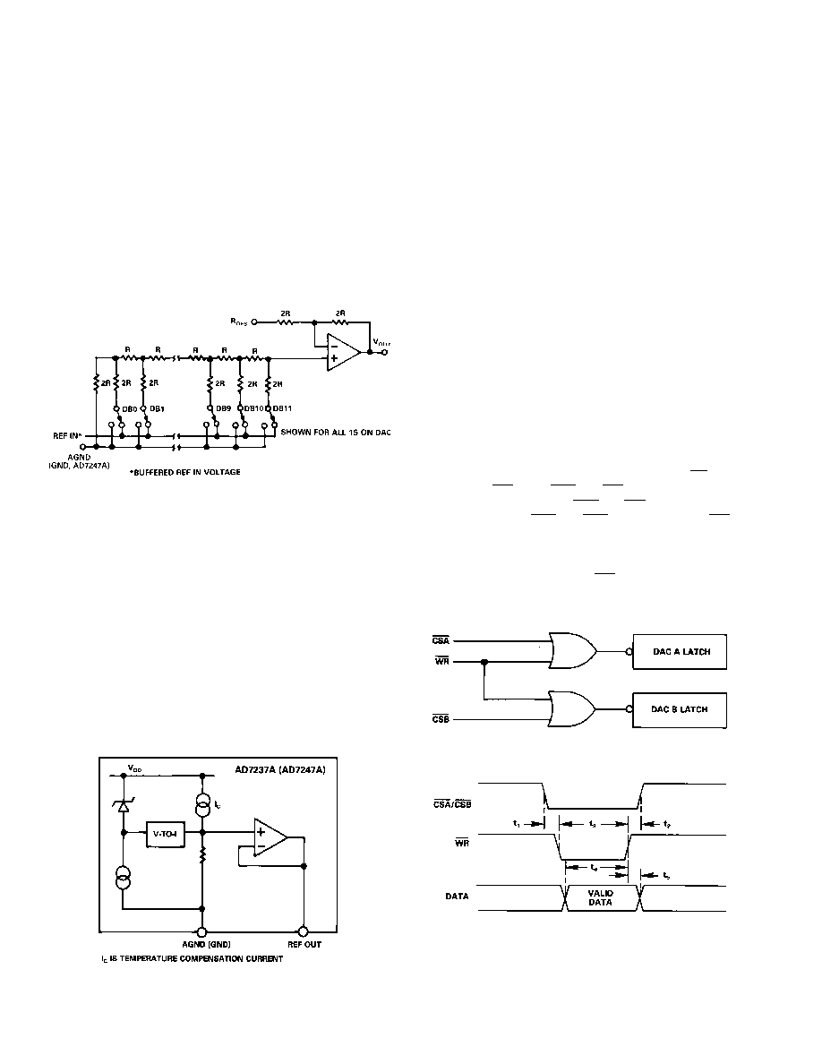
INTERFACE LOGIC INFORMATION—AD7247A
Table I shows the truth table for AD7247A operation. The part
contains a single, parallel 12-bit latch for each DAC. It can be
treated as two independent DACs, each with its own CS input
and a common WR input. CSA and WR control the loading of
data to the DAC A latch while CSB and WR control the loading
of the DAC B latch. If CSA and CSB are both low, with WR
low, the same data will be written to both DAC latches. All con-
trol signals are level triggered and therefore either or both
latches can be made transparent. Input data is latched to the re-
spective latch on the rising edge of WR. Figure 4 shows the in-
put control logic for the AD7247A, while the write cycle timing
diagram for the part is shown in Figure 5.
Figure 4. AD7247A Input Control Logic
Figure 5. AD7247A Write Cycle Timing Diagram
相关PDF资料 |
PDF描述 |
|---|---|
| VI-26T-IV | CONVERTER MOD DC/DC 6.5V 150W |
| VI-BNP-MU-S | CONVERTER MOD DC/DC 13.8V 200W |
| VI-26M-IV | CONVERTER MOD DC/DC 10V 150W |
| AD5390BSTZ-3 | IC DAC 14BIT 16CHAN 3V 52LQFP |
| AD5390BSTZ-5 | IC DAC 14BIT I2C 16CH 52-LQFP |
相关代理商/技术参数 |
参数描述 |
|---|---|
| AD7237ATQ | 功能描述:数模转换器- DAC IMPROVED 12-BIT DACPORT RoHS:否 制造商:Texas Instruments 转换器数量:1 DAC 输出端数量:1 转换速率:2 MSPs 分辨率:16 bit 接口类型:QSPI, SPI, Serial (3-Wire, Microwire) 稳定时间:1 us 最大工作温度:+ 85 C 安装风格:SMD/SMT 封装 / 箱体:SOIC-14 封装:Tube |
| AD7237ATQ/883B | 制造商:未知厂家 制造商全称:未知厂家 功能描述:12-Bit Digital-to-Analog Converter |
| AD7237BQ | 制造商:Rochester Electronics LLC 功能描述:- Bulk |
| AD7237JN | 制造商:Analog Devices 功能描述:DAC 2-CH R-2R 12-bit 24-Pin PDIP Tube 制造商:Rochester Electronics LLC 功能描述:DUAL 12 BIT DAC PORT IC - Bulk 制造商:Analog Devices 功能描述:IC 12BIT DAC 7237 DIP24 |
| AD7237JNZ | 功能描述:IC DAC 12BIT LC2MOS DUAL 24-DIP RoHS:是 类别:集成电路 (IC) >> 数据采集 - 数模转换器 系列:DACPORT® 标准包装:1 系列:- 设置时间:4.5µs 位数:12 数据接口:串行,SPI? 转换器数目:1 电压电源:单电源 功率耗散(最大):- 工作温度:-40°C ~ 125°C 安装类型:表面贴装 封装/外壳:8-SOIC(0.154",3.90mm 宽) 供应商设备封装:8-SOICN 包装:剪切带 (CT) 输出数目和类型:1 电压,单极;1 电压,双极 采样率(每秒):* 其它名称:MCP4921T-E/SNCTMCP4921T-E/SNRCTMCP4921T-E/SNRCT-ND |
发布紧急采购,3分钟左右您将得到回复。