参数资料
| 型号: | AD7237KN |
| 厂商: | Analog Devices Inc |
| 文件页数: | 8/12页 |
| 文件大小: | 0K |
| 描述: | IC DAC 12BIT LC2MOS DUAL 24-DIP |
| 产品培训模块: | Data Converter Fundamentals DAC Architectures |
| 标准包装: | 15 |
| 系列: | DACPORT® |
| 设置时间: | 8µs |
| 位数: | 12 |
| 数据接口: | 并联 |
| 转换器数目: | 2 |
| 电压电源: | 双 ± |
| 工作温度: | -40°C ~ 85°C |
| 安装类型: | 通孔 |
| 封装/外壳: | 24-DIP(0.300",7.62mm) |
| 供应商设备封装: | 24-PDIP |
| 包装: | 管件 |
| 输出数目和类型: | 2 电压,单极;2 电压,双极 |
| 采样率(每秒): | * |
AD7237A/AD7247A
REV. 0
–5–
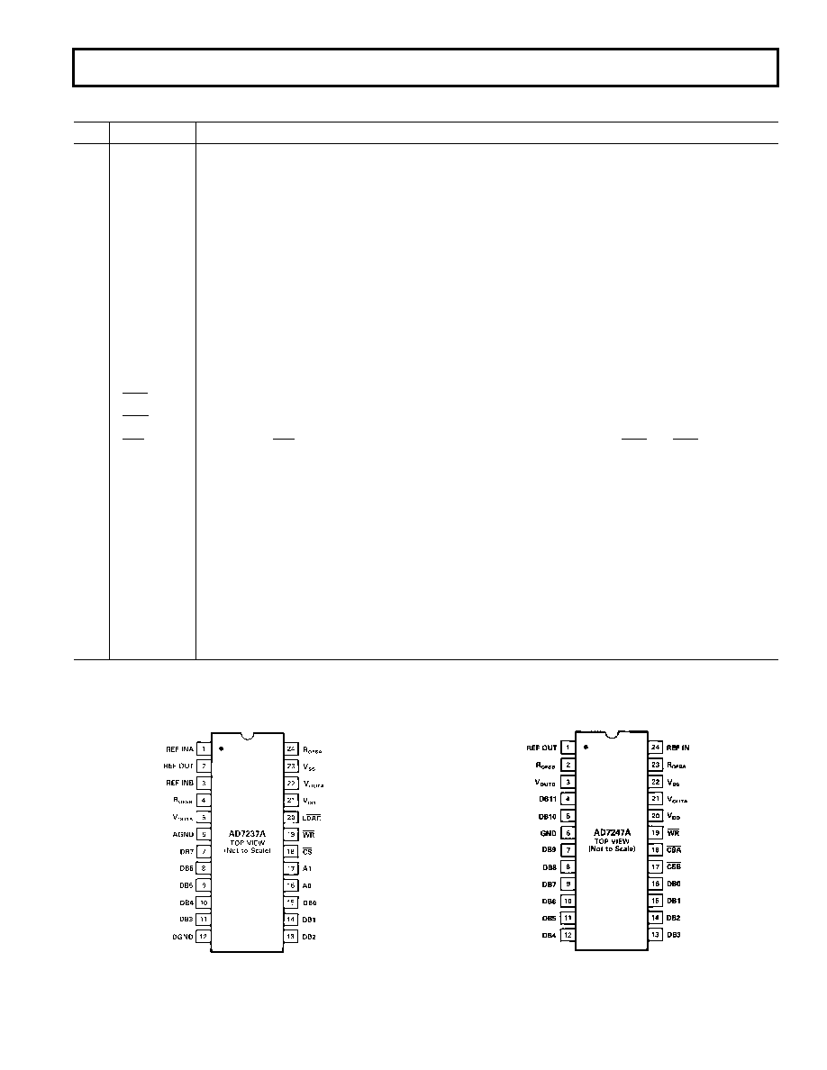
AD7247A PIN FUNCTION DESCRIPTION (DIP PIN NUMBERS)
Pin
Mnemonic
Description
1
REF OUT
Voltage Reference Output. The internal 5 V analog reference is provided at this pin. To operate the part
with internal reference, REF OUT should be connected to REF IN.
2ROFSB
Output Offset Resistor for DAC B. This input configures the output ranges for DAC B. It is connected to
VOUTB for the +5 V range, to GND for the +10 V range and to REF IN for the ± 5 V range.
3VOUTB
Analog Output Voltage from DAC B. This is the buffer amplifier output voltage. Three different output
voltage ranges can be chosen: 0 V to +5 V, 0 V to +10 V and
±5 V. The amplifier is capable of developing
+10 V across a 2 k
resistor to GND.
4
DB11
Data Bit 11 (MSB).
5
DB10
Data Bit 10.
6
GND
Ground. Ground reference for all on-chip circuitry.
7–15
DB9-DB1
Data Bit 9 to Data Bit 1.
16
DB0
Data Bit 0 (LSB).
17
CSB
Chip Select Input for DAC B. Active low logic input. DAC B is selected when this input is active.
18
CSA
Chip Select Input for DAC A. Active low logic input. DAC A is selected when this input is active.
19
WR
Write Input. WR is an active low logic input which is used in conjunction with CSA and CSB to write data
to the DAC latches.
20
VDD
Positive Supply (+12 V to +15 V).
21
VOUTA
Analog Output Voltage from DAC A. This is the buffer amplifier output voltage. Three different output
voltage ranges can be chosen: 0 V to +5 V, 0 V to +10 V and
±5 V. The amplifier is capable of developing
+10 V across a 2 k
resistor to GND.
22
VSS
Negative Supply (0 V or –12 V to –15 V).
23
ROFSA
Output Offset Resistor for DAC A. This input configures the output ranges for DAC A. It is connected to
VOUTA for the +5 V range, to GND for the +10 V range and to REF IN for the
±5 V range.
24
REF IN
Voltage Reference Input. The common reference voltage for both DACs is applied to this pin. It is internally
buffered before being applied to both DACs. The nominal reference voltage for correct operation of the
AD7247A is 5 V.
AD7237A PIN CONFIGURATION
DIP and SOIC
AD7247A PIN CONFIGURATION
DIP and SOIC
相关PDF资料 |
PDF描述 |
|---|---|
| AD5363BCPZ | IC DAC 14BIT 8CH SERIAL 56-LFCSP |
| LTC1596AISW#TRPBF | IC D/A CONV 16BIT MLTPLYNG16SOIC |
| LTC1596AISW#TR | IC DAC 16BIT MULTIPLY SER 16SOIC |
| LTC1596-1AISW#TRPBF | IC D/A CONV 16BIT MLTPLYNG16SOIC |
| LTC1596-1AISW#TR | IC DAC 16BIT MULTIPLY SER 16SOIC |
相关代理商/技术参数 |
参数描述 |
|---|---|
| AD7237KNZ | 制造商:Analog Devices 功能描述: |
| AD7237KP | 制造商:未知厂家 制造商全称:未知厂家 功能描述:12-Bit Digital-to-Analog Converter |
| AD7237KR | 功能描述:IC DAC 12BIT W/AMP W/BUFF 24SOIC RoHS:否 类别:集成电路 (IC) >> 数据采集 - 数模转换器 系列:DACPORT® 产品培训模块:Data Converter Fundamentals DAC Architectures 标准包装:750 系列:- 设置时间:7µs 位数:16 数据接口:并联 转换器数目:1 电压电源:双 ± 功率耗散(最大):100mW 工作温度:0°C ~ 70°C 安装类型:表面贴装 封装/外壳:28-LCC(J 形引线) 供应商设备封装:28-PLCC(11.51x11.51) 包装:带卷 (TR) 输出数目和类型:1 电压,单极;1 电压,双极 采样率(每秒):143k |
| AD7237KR-REEL | 制造商:Analog Devices 功能描述:DAC 2-CH R-2R 12-bit 24-Pin SOIC W T/R 制造商:Analog Devices 功能描述:DAC 2CH R-2R 12-BIT 24SOIC W - Tape and Reel |
| AD7237KRZ | 功能描述:IC DAC 12BIT DL AMP/BUFF 24SOIC RoHS:是 类别:集成电路 (IC) >> 数据采集 - 数模转换器 系列:DACPORT® 产品培训模块:Data Converter Fundamentals DAC Architectures 标准包装:750 系列:- 设置时间:7µs 位数:16 数据接口:并联 转换器数目:1 电压电源:双 ± 功率耗散(最大):100mW 工作温度:0°C ~ 70°C 安装类型:表面贴装 封装/外壳:28-LCC(J 形引线) 供应商设备封装:28-PLCC(11.51x11.51) 包装:带卷 (TR) 输出数目和类型:1 电压,单极;1 电压,双极 采样率(每秒):143k |
发布紧急采购,3分钟左右您将得到回复。