参数资料
| 型号: | AD7243AR |
| 厂商: | Analog Devices Inc |
| 文件页数: | 11/12页 |
| 文件大小: | 0K |
| 描述: | IC SRL DAC 12BIT LC2MOS 16-SOIC |
| 产品培训模块: | Data Converter Fundamentals DAC Architectures |
| 标准包装: | 47 |
| 系列: | DACPORT® |
| 设置时间: | 10µs |
| 位数: | 12 |
| 数据接口: | 串行 |
| 转换器数目: | 1 |
| 电压电源: | 双 ± |
| 功率耗散(最大): | 100mW |
| 工作温度: | -40°C ~ 85°C |
| 安装类型: | 表面贴装 |
| 封装/外壳: | 16-SOIC(0.295",7.50mm 宽) |
| 供应商设备封装: | 16-SOIC W |
| 包装: | 管件 |
| 输出数目和类型: | 1 电压,单极;1 电压,双极 |
| 采样率(每秒): | 300k |
AD7243
–8–
REV. A
APPLYING THE AD7243
Power Supply Decoupling
To achieve optimum performance when using the AD7243, the
VDD and VSS lines should each be decoupled to DGND using
0.1
F capacitors. In noisy environments it is recommended
that 10
F capacitors be connected in parallel with the 0.1 F
capacitors.
The internal scaling resistors provided on the AD7243 allow
several output voltage ranges. The part can produce unipolar
output ranges of 0 V to +5 V or 0 V to +10 V and a bipolar out-
put range of
±5 V. Connections for the various ranges are out-
lined below.
Unipolar (0 V to +10 V) Configuration
The first of the configurations provides an output voltage range
of 0 V to +10 V. This is achieved by connecting the output off-
set resistor ROFS (Pin 13) to AGND. Natural Binary data format
is selected by connecting
BIN/COMP (Pin 4) to DGND. In this
configuration, the AD7243 can be operated using either single
or dual supplies. Note that the VDD supply must be
≥+14.25 V
for this range in order to maintain sufficient amplifier head-
room. Dual supplies may be used to improve settling time and
give increased current sink capability for the amplifier. Figure 9
shows the connection diagram for unipolar operation of the
AD7243. Table I shows the digital code vs. analog output for
this configuration.
DAC
AGND
DGND
REFOUT
REFIN
ROFS
VOUT
VDD
2R
AD7243*
BIN/
COMP
0V OR VSS
0V TO + 10V
*ADDITIONAL PINS OMITTED FOR CLARITY
VDD
VSS
Figure 9. Unipolar (0 V to +10 V) Configuration
Table I. Unipolar Code Table (0 V to +10 V Range)
Input Data Word
MSB
LSB
Analog Output, VOUT
XXXX 1111 1111 1111
+2 REFIN
× (4095/4096)
XXXX 1000 0000 0001
+2 REFIN
× (2049/4096)
XXXX 1000 0000 0000
+2 REFIN
× (2048/4096)= +REFIN
XXXX 0111 1111 1111
+2 REFIN
× (2047/4096)
XXXX 0000 0000 0001
+2 REFIN
× (1/4096)
XXXX 0000 0000 0000
0 V
X = Don’t Care.
Note: 1 LSB = 2 REFIN/4096.
Unipolar (0 V to +5 V) Configuration
The 0 V to +5 V output voltage range is achieved by connecting
ROFS to VOUT. Once again, the AD7243 can be operated using
either single or dual supplies. The table for output voltage vs.
digital code is as in Table I, with 2REFIN replaced by REFIN.
Note, for this range, 1 LSB = REFIN (2
–12 ) = (REFIN/4096).
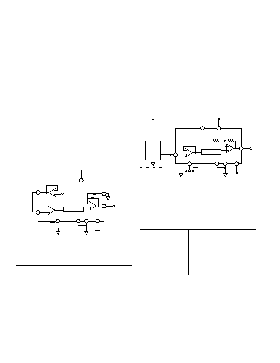
Bipolar ( 5 V) Configuration
The bipolar configuration for the AD7243, which gives an out-
put range of –5 V to +5 V, is achieved by connecting ROFS to
REFIN. The AD7243 must be operated from dual supplies to
achieve this output voltage range. Either offset binary or two’s
complement data format may be selected. Figure 10 shows the
connection diagram for bipolar operation. An AD586 provides
the reference voltage for the DAC but this could be provided by
the on-chip reference by connecting REFOUT to REFIN.
VDD
DAC
AGND
DGND
REFIN
ROFS
2R
AD7243*
BIN/ COMP
–5V TO + 5V
*ADDITIONAL PINS OMITTED FOR CLARITY
AD586
GND
+VIN
VOUT
VDD
VSS
VOUT
VDD
Figure 10. Bipolar Configuration with External Reference
Bipolar Operation (Two’s Complement Data Format)
The AD7243 is configured for two’s complement data format
by connecting
BIN/COMP (Pin 4) high. The analog output vs.
digital code is shown in Table II.
Table II. Two’s Complement Bipolar Code Table
Input Data Word
MSB
LSB
Analog Output, VOUT
XXXX 0111 1111 1111
+REFIN
× (2047/2048)
XXXX 0000 0000 0001
+REFIN
× (1/2048)
XXXX 0000 0000 0000
0 V
XXXX 1111 1111 1111
–REFIN
× (1/2048)
XXXX 1000 0000 0001
–REFIN
× (2047/2048)
XXXX 1000 0000 0000
–REFIN
× (2048/2048) = –REFIN
X = Don’t Care.
Note: 1 LSB = REFIN/2048.
Bipolar Operation (Offset Binary Data Format)
The AD7243 is configured for Offset Binary data format by
connecting
BIN/COMP (Pin 4) low. The analog output vs. digi-
tal code may be obtained by inverting the MSB in Table II.
相关PDF资料 |
PDF描述 |
|---|---|
| ADA4960-1ACPZ-RL | IC ADC DRIVER DIFF 16LFCSP |
| VE-25N-IV-F3 | CONVERTER MOD DC/DC 18.5V 150W |
| LTC6405CMS8E#PBF | IC AMP/DRVR DIFF R-R 5V 8-MSOP |
| SY88843VMG | IC AMP LIMIT CML TTL SD 16MLF |
| VE-2TM-IV-F1 | CONVERTER MOD DC/DC 10V 150W |
相关代理商/技术参数 |
参数描述 |
|---|---|
| AD7243AR-REEL | 功能描述:IC DAC 12BIT W/AMP W/REF 16-SOIC RoHS:否 类别:集成电路 (IC) >> 数据采集 - 数模转换器 系列:DACPORT® 标准包装:47 系列:- 设置时间:2µs 位数:14 数据接口:并联 转换器数目:1 电压电源:单电源 功率耗散(最大):55µW 工作温度:-40°C ~ 85°C 安装类型:表面贴装 封装/外壳:28-SSOP(0.209",5.30mm 宽) 供应商设备封装:28-SSOP 包装:管件 输出数目和类型:1 电流,单极;1 电流,双极 采样率(每秒):* |
| AD7243ARZ | 功能描述:IC DAC 12BIT W/AMP W/REF 16-SOIC RoHS:是 类别:集成电路 (IC) >> 数据采集 - 数模转换器 系列:DACPORT® 产品培训模块:Lead (SnPb) Finish for COTS Obsolescence Mitigation Program 标准包装:50 系列:- 设置时间:4µs 位数:12 数据接口:串行 转换器数目:2 电压电源:单电源 功率耗散(最大):- 工作温度:-40°C ~ 85°C 安装类型:表面贴装 封装/外壳:8-TSSOP,8-MSOP(0.118",3.00mm 宽) 供应商设备封装:8-uMAX 包装:管件 输出数目和类型:2 电压,单极 采样率(每秒):* 产品目录页面:1398 (CN2011-ZH PDF) |
| AD7243ARZ | 制造商:Analog Devices 功能描述:IC, DAC, 12BIT, 300KSPS, SOIC-16 |
| AD7243ARZ-REEL | 功能描述:IC SRL DAC 12BIT LC2MOS 16-SOIC RoHS:是 类别:集成电路 (IC) >> 数据采集 - 数模转换器 系列:DACPORT® 标准包装:47 系列:- 设置时间:2µs 位数:14 数据接口:并联 转换器数目:1 电压电源:单电源 功率耗散(最大):55µW 工作温度:-40°C ~ 85°C 安装类型:表面贴装 封装/外壳:28-SSOP(0.209",5.30mm 宽) 供应商设备封装:28-SSOP 包装:管件 输出数目和类型:1 电流,单极;1 电流,双极 采样率(每秒):* |
| AD7243BN | 功能描述:IC DAC 12BIT W/AMP W/REF 16-DIP RoHS:否 类别:集成电路 (IC) >> 数据采集 - 数模转换器 系列:DACPORT® 产品培训模块:Data Converter Fundamentals DAC Architectures 标准包装:750 系列:- 设置时间:7µs 位数:16 数据接口:并联 转换器数目:1 电压电源:双 ± 功率耗散(最大):100mW 工作温度:0°C ~ 70°C 安装类型:表面贴装 封装/外壳:28-LCC(J 形引线) 供应商设备封装:28-PLCC(11.51x11.51) 包装:带卷 (TR) 输出数目和类型:1 电压,单极;1 电压,双极 采样率(每秒):143k |
发布紧急采购,3分钟左右您将得到回复。