- 您现在的位置:买卖IC网 > PDF目录373895 > AD7243BN (ANALOG DEVICES INC) 47 UF, 20V CAP., TANTALUM PDF资料下载
参数资料
| 型号: | AD7243BN |
| 厂商: | ANALOG DEVICES INC |
| 元件分类: | DAC |
| 英文描述: | 47 UF, 20V CAP., TANTALUM |
| 中文描述: | SERIAL INPUT LOADING, 5 us SETTLING TIME, 12-BIT DAC, PDIP16 |
| 封装: | PLASTIC, DIP-16 |
| 文件页数: | 10/12页 |
| 文件大小: | 171K |
| 代理商: | AD7243BN |
AD7243
–10–
REV. A
AD7243–87C51 Interface
A serial interface between the AD7243 and the 87C51
microcontroller is shown in Figure 14. TXD of the 87C51 drives
SCLK of the AD7243, while RXD drives the serial data line of
the part. The
SYNC
signal is derived from the port line P3.3.
The 87C51 provides the LSB of its SBUF register as the first bit
in the serial data stream. Therefore, the user will have to ensure
that the data in the SBUF register is arranged correctly so that
the don’t care bits are the first to be transmitted to the AD7243
and the last bit to be sent is the LSB of the word to be loaded to
the AD7243. When data is to be transmitted to the part, P3.3 is
taken low. Data on RXD is valid on the falling edge of TXD.
The 87C51 transmits its serial data in 8-bit bytes with only eight
falling clock edges occurring in the transmit cycle. To load data
to the AD7243, P3.3 is left low after the first eight bits are trans-
ferred and a second byte of data is then transferred serially to the
AD7243. When the second serial transfer is complete, the P3.3
line is taken high.
Figure 14 shows the
LDAC
input of the AD7243 hard wired
low. As a result, the DAC latch and the analog output will be up-
dated on the sixteenth falling edge of TXD after the
SYNC
sig-
nal for the DAC has gone low. Alternatively, the scheme used in
previous interfaces, whereby the
LDAC
input is driven from a
timer, can be used.
LDAC
SCLK
SDIN
AD7243*
SYNC
*ADDITIONAL PINS OMITTED FOR CLARITY
P3.3
TXD
RXD
87C51*
Figure 14. AD7243–87C51 Interface
AD7243–68HC11 Interface
Figure 15 shows a serial interface between the AD7243 and the
68HC11 microcontroller. SCK of the 68HC11 drives SCLK of
the AD7243 while the MOSI output drives the serial data line of
the AD7243. The
SYNC
signal is derived from a port line (PC7
shown).
For correct operation of this interface, the 68HC11 should be
configured such that its CPOL bit is a 0 and its CPHA bit is a 1.
When data is to be transmitted to the part, PC7 is taken low.
When the 68HC11 is configured like this, data on MOSI is valid
on the falling edge of SCK. The 68HC11 transmits its serial data
in 8-bit bytes with only eight falling clock edges occurring in the
transmit cycle. To load data to the AD7243, PC7 is left low after
the first eight bits are transferred and a second byte of data is
then transferred serially to the AD7243. When the second serial
transfer is complete, the PC7 line is taken high.
Figure 15 shows the
LDAC
input of the AD7243 hardwired
low. As a result, the DAC latch and the analog output of the
DAC will be updated on the sixteenth falling edge of SCK after
the respective
SYNC
signal has gone low. Alternatively, the
scheme used in previous interfaces, whereby the
LDAC
input is
driven from a timer, can be used.
LDAC
SCLK
SDIN
AD7243*
SYNC
*ADDITIONAL PINS OMITTED FOR CLARITY
PC7
SCK
MOSI
68HC11*
Figure 15. AD7243–68HC11 Interface
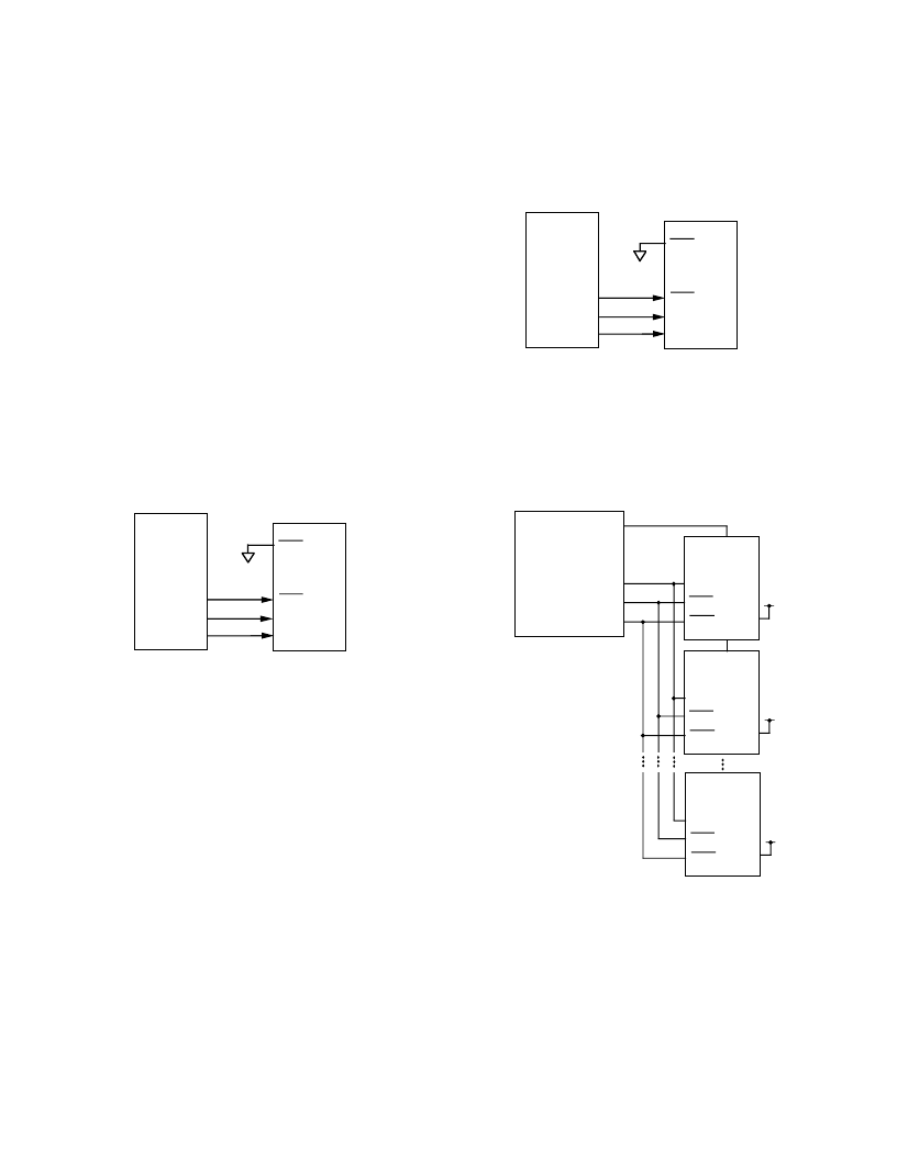
Multiple DAC Daisy-Chain Interface
A multi-DAC serial interface is shown in Figure 16. This
scheme may be used with all of the interfaces previously dis-
cussed if more than one DAC is required in a system. To enable
the facility the DCEN pin must be connected high on all de-
vices, including the last device in the chain.
SCLK
AD7243*
SYNC
LDAC
*ADDITIONAL PINS OMITTED FOR CLARITY
PA1
PA2
PA3
MICROCONTROLLER
PA0
SDIN
DCEN
SDO
SCLK
AD7243*
SYNC
LDAC
SDIN
DCEN
SDO
SCLK
AD7243*
SYNC
LDAC
SDIN
DCEN
SDO
V
DD
V
DD
V
DD
Figure 16. AD7243 Daisy-Chain Configuration
相关PDF资料 |
PDF描述 |
|---|---|
| AD7243BQ | LC2MOS 12-Bit Serial DACPORT |
| AD7243BR | SM IC/74HC08 SO-14 QUAD 2-IN |
| AD7243SQ2 | LC2MOS 12-Bit Serial DACPORT |
| AD7247A | LC2MOS Dual 12-Bit DACPORTs |
| AD7237A | LC2MOS Dual 12-Bit DACPORTs |
相关代理商/技术参数 |
参数描述 |
|---|---|
| AD7243BNZ | 功能描述:IC DAC 12BIT AMP/REF 16DIP RoHS:是 类别:集成电路 (IC) >> 数据采集 - 数模转换器 系列:DACPORT® 标准包装:1 系列:- 设置时间:4.5µs 位数:12 数据接口:串行,SPI? 转换器数目:1 电压电源:单电源 功率耗散(最大):- 工作温度:-40°C ~ 125°C 安装类型:表面贴装 封装/外壳:8-SOIC(0.154",3.90mm 宽) 供应商设备封装:8-SOICN 包装:剪切带 (CT) 输出数目和类型:1 电压,单极;1 电压,双极 采样率(每秒):* 其它名称:MCP4921T-E/SNCTMCP4921T-E/SNRCTMCP4921T-E/SNRCT-ND |
| AD7243BQ | 功能描述:IC DAC 12BIT W/AMP W/REF 16-CDIP RoHS:否 类别:集成电路 (IC) >> 数据采集 - 数模转换器 系列:DACPORT® 产品培训模块:Data Converter Fundamentals DAC Architectures 标准包装:750 系列:- 设置时间:7µs 位数:16 数据接口:并联 转换器数目:1 电压电源:双 ± 功率耗散(最大):100mW 工作温度:0°C ~ 70°C 安装类型:表面贴装 封装/外壳:28-LCC(J 形引线) 供应商设备封装:28-PLCC(11.51x11.51) 包装:带卷 (TR) 输出数目和类型:1 电压,单极;1 电压,双极 采样率(每秒):143k |
| AD7243BR | 功能描述:IC DAC 12BIT W/AMP W/REF 16-SOIC RoHS:否 类别:集成电路 (IC) >> 数据采集 - 数模转换器 系列:DACPORT® 产品培训模块:Data Converter Fundamentals DAC Architectures 标准包装:750 系列:- 设置时间:7µs 位数:16 数据接口:并联 转换器数目:1 电压电源:双 ± 功率耗散(最大):100mW 工作温度:0°C ~ 70°C 安装类型:表面贴装 封装/外壳:28-LCC(J 形引线) 供应商设备封装:28-PLCC(11.51x11.51) 包装:带卷 (TR) 输出数目和类型:1 电压,单极;1 电压,双极 采样率(每秒):143k |
| AD7243BR-REEL | 功能描述:IC DAC 12BIT W/AMP W/REF 16-SOIC RoHS:否 类别:集成电路 (IC) >> 数据采集 - 数模转换器 系列:DACPORT® 产品培训模块:Data Converter Fundamentals DAC Architectures 标准包装:750 系列:- 设置时间:7µs 位数:16 数据接口:并联 转换器数目:1 电压电源:双 ± 功率耗散(最大):100mW 工作温度:0°C ~ 70°C 安装类型:表面贴装 封装/外壳:28-LCC(J 形引线) 供应商设备封装:28-PLCC(11.51x11.51) 包装:带卷 (TR) 输出数目和类型:1 电压,单极;1 电压,双极 采样率(每秒):143k |
| AD7243BRZ | 功能描述:IC DAC 12BIT SRL LC2MOS 16SOIC RoHS:是 类别:集成电路 (IC) >> 数据采集 - 数模转换器 系列:DACPORT® 产品培训模块:Lead (SnPb) Finish for COTS Obsolescence Mitigation Program 标准包装:50 系列:- 设置时间:4µs 位数:12 数据接口:串行 转换器数目:2 电压电源:单电源 功率耗散(最大):- 工作温度:-40°C ~ 85°C 安装类型:表面贴装 封装/外壳:8-TSSOP,8-MSOP(0.118",3.00mm 宽) 供应商设备封装:8-uMAX 包装:管件 输出数目和类型:2 电压,单极 采样率(每秒):* 产品目录页面:1398 (CN2011-ZH PDF) |
发布紧急采购,3分钟左右您将得到回复。