- 您现在的位置:买卖IC网 > PDF目录373895 > AD7244 (Analog Devices, Inc.) LC2MOS Dual, Complete, 12-Bit/14-Bit Serial DACs PDF资料下载
参数资料
| 型号: | AD7244 |
| 厂商: | Analog Devices, Inc. |
| 英文描述: | LC2MOS Dual, Complete, 12-Bit/14-Bit Serial DACs |
| 中文描述: | LC2MOS双,完整,12-Bit/14-Bit串行数模转换器 |
| 文件页数: | 10/12页 |
| 文件大小: | 319K |
| 代理商: | AD7244 |
AD7242/AD7244
REV. A
–10–
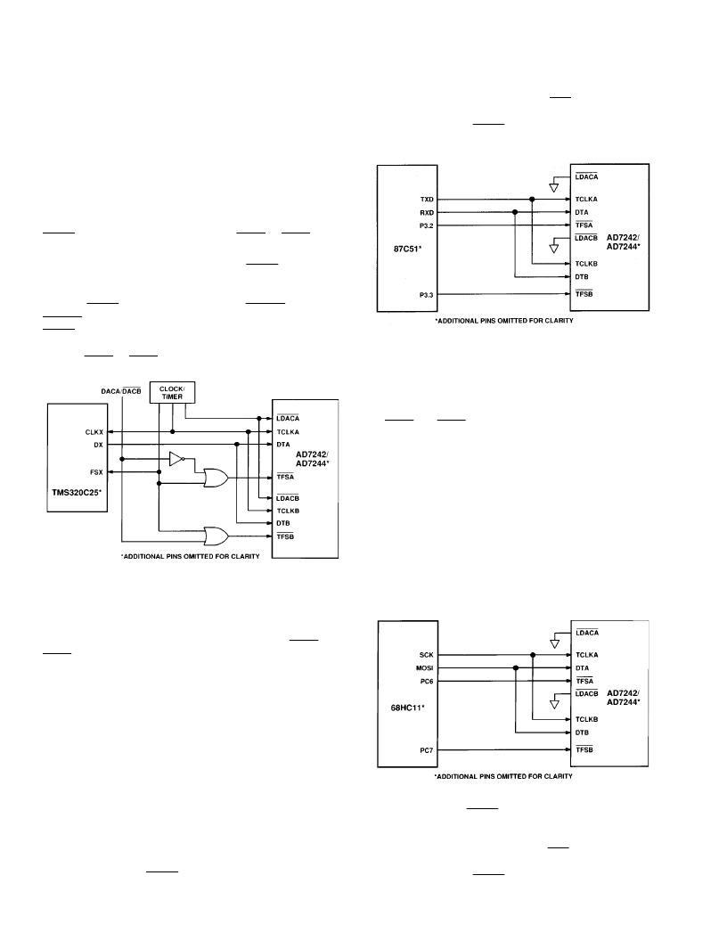
AD7242/AD7244 to TMS320C25 Interface
Figure 9 shows a serial interface between the AD7242/AD7244
and the TMS320C25 DSP processor. In this interface, the
CLKX and FSX signals of the TMS320C25 are generated from
the clock/timer circuitry. The FSX pin of the TMS320C25
must be configured as an input. CLKX is used to provide both
the TCLKA and TCLKB inputs of the AD7242/AD7244. DX
of the TMS320C25 is also routed to the serial data line of each
input port of the AD7242/AD7244.
Data from the TMS32020 is valid on the falling edge of CLKX
after FSX goes low. This FSX signal is gated with the DACA/
DACB
control line to determine whether
TFSA
or
TFSB
goes
low when FSX goes low.
The clock/timer circuitry also generates the
LDAC
signal for the
AD7242/AD7244 to synchronize the update of the outputs with
the serial transmission. As in the previous interface diagrams, a
common
LDAC
input is shown driving the
LDACA
and
LDACB
inputs of the AD7242/AD7244. Once again, these
LDAC
inputs could be hardwired low, in which case V
OUTA
or
V
OUTB
will be updated on the sixteenth falling edge of CLKX
after the
TFSA
or
TFSB
input goes low.
Figure 9. AD7242/AD7244 to TMS320C25 Interface
AD7242/AD7244 to 87C51 Interface
A serial interface between the AD7242/AD7244 and the 87C51
microcontroller is shown in Figure 10. TXD of the 87C51
drives TCLKA and TCLKB of the AD7242/AD7244 while
RXD drives the two serial data lines of the part. The
TFSA
and
TFSB
signals are derived from P3.2 and P3.3, respectively.
The 87C51 provides the LSB of its SBUF register as the first bit
in the serial data stream. Therefore, the user will have to ensure
that the data in the SBUF register is correctly arranged so the
don’t care bits are the first to be transmitted to the AD7242/
AD7244; the last bit to be sent is the LSB of the word to be
loaded to the AD7242/AD7244. When data is to be transmitted
to the part, P3.2 (for DACA) or P3.3 (for DACB) is taken low.
Data on RXD is valid on the falling edge of TXD. The 87C51
transmits its serial data in 8-bit bytes with only eight falling
clock edges occurring in the transmit cycle. To load data to the
AD7242/AD7244, P3.2 (for DACA) or P3.3 (for DACB) is left
low after the first eight bits are transferred and a second byte of
data is then serially transferred to the AD7242/AD7244. When
the second serial transfer is complete, the P3.2 line (for DACA)
or the P3.3 line (for DACB) is taken high.
Figure 10 shows both
LDAC
inputs of the AD7242/AD7244
hardwired low. As a result, the DAC latch and the analog
output of one of the DACs will be updated on the sixteenth
falling edge of TXD after the respective
TFS
signal for that
DAC has gone low. Alternatively, the scheme used in previous
interfaces, whereby the
LDAC
inputs are driven from a timer,
can be used.
Figure 10. AD7242/AD7244 to 87C51 Interface
AD7242/AD7244 to 68HC11 Interface
Figure 11 shows a serial interface between the AD7242/AD7244
and the 68HC11 microcontroller. SCK of the 68HC11 drives
TCLKA and TCLKB of the AD7242/AD7244 while the MOSI
output drives the two serial data lines of the AD7242/AD7244.
The
TFSA
and
TFSB
signals are derived from PC6 and PC7,
respectively.
For correct operation of this interface, the 68HC11 should be
configured such that its CPOL bit is a 0 and its CPHA bit is a 1.
When data is to be transmitted to the part, PC6 (for DACA) or
PC7 (for DACB) is taken low. When the 68HC11 is configured
like this, data on MOSI is valid on the falling edge of SCK. The
68HCll transmits its serial data in 8-bit bytes with only eight
falling clock edges occurring in the transmit cycle. To load data
to the AD7242/AD7244, PC6 (for DACA) or PC7 (for DACB)
is left low after the first eight bits are transferred and a second
byte of data is then serially transferred to the AD7242/AD7244.
When the second serial transfer is complete, the PC6 line (for
DACA) or the PC7 line (for DACB) is taken high.
Figure 11. AD7242/AD7244 to 68HC11 Interface
Figure 11 shows both
LDAC
inputs of the AD7242/AD7244
hardwired low. As a result, the DAC latch and the analog
output of one of the DACs will be updated on the sixteenth
falling edge of SCK after the respective
TFS
signal for that
DAC has gone low. Alternatively, the scheme used in previous
interfaces, whereby the
LDAC
inputs are driven from a timer,
can be used.
相关PDF资料 |
PDF描述 |
|---|---|
| AD7244AQ | LC2MOS Dual, Complete, 12-Bit/14-Bit Serial DACs |
| AD7242JN | LC2MOS Dual, Complete, 12-Bit/14-Bit Serial DACs |
| AD7243 | LC2MOS 12-Bit Serial DACPORT |
| AD7243AN | LC2MOS 12-Bit Serial DACPORT |
| AD7243AQ | LC2MOS 12-Bit Serial DACPORT |
相关代理商/技术参数 |
参数描述 |
|---|---|
| AD7244AQ | 功能描述:IC DAC 14BIT SRL W/REF 24-CDIP RoHS:否 类别:集成电路 (IC) >> 数据采集 - 数模转换器 系列:- 产品培训模块:Lead (SnPb) Finish for COTS Obsolescence Mitigation Program 标准包装:1,000 系列:- 设置时间:1µs 位数:8 数据接口:串行 转换器数目:8 电压电源:双 ± 功率耗散(最大):941mW 工作温度:0°C ~ 70°C 安装类型:表面贴装 封装/外壳:24-SOIC(0.295",7.50mm 宽) 供应商设备封装:24-SOIC W 包装:带卷 (TR) 输出数目和类型:8 电压,单极 采样率(每秒):* |
| AD7244JN | 功能描述:IC DAC 14BIT SRL W/REF 24-DIP RoHS:否 类别:集成电路 (IC) >> 数据采集 - 数模转换器 系列:- 标准包装:2,400 系列:- 设置时间:- 位数:18 数据接口:串行 转换器数目:3 电压电源:模拟和数字 功率耗散(最大):- 工作温度:-40°C ~ 85°C 安装类型:表面贴装 封装/外壳:36-TFBGA 供应商设备封装:36-TFBGA 包装:带卷 (TR) 输出数目和类型:* 采样率(每秒):* |
| AD7244JNZ | 功能描述:IC DAC 14BIT SERIAL W/REF 24DIP RoHS:是 类别:集成电路 (IC) >> 数据采集 - 数模转换器 系列:- 标准包装:1 系列:- 设置时间:4.5µs 位数:12 数据接口:串行,SPI? 转换器数目:1 电压电源:单电源 功率耗散(最大):- 工作温度:-40°C ~ 125°C 安装类型:表面贴装 封装/外壳:8-SOIC(0.154",3.90mm 宽) 供应商设备封装:8-SOICN 包装:剪切带 (CT) 输出数目和类型:1 电压,单极;1 电压,双极 采样率(每秒):* 其它名称:MCP4921T-E/SNCTMCP4921T-E/SNRCTMCP4921T-E/SNRCT-ND |
| AD7244JR | 功能描述:IC DAC 14BIT LC2MOS DUAL 28SOIC RoHS:否 类别:集成电路 (IC) >> 数据采集 - 数模转换器 系列:- 产品培训模块:Lead (SnPb) Finish for COTS Obsolescence Mitigation Program 标准包装:1,000 系列:- 设置时间:1µs 位数:8 数据接口:串行 转换器数目:8 电压电源:双 ± 功率耗散(最大):941mW 工作温度:0°C ~ 70°C 安装类型:表面贴装 封装/外壳:24-SOIC(0.295",7.50mm 宽) 供应商设备封装:24-SOIC W 包装:带卷 (TR) 输出数目和类型:8 电压,单极 采样率(每秒):* |
| AD7244JR-REEL | 制造商:Rochester Electronics LLC 功能描述:- Tape and Reel |
发布紧急采购,3分钟左右您将得到回复。