- 您现在的位置:买卖IC网 > PDF目录165342 > AD7244JNZ (ANALOG DEVICES INC) 12-/14-Bit DAC, 3 V Buried Zener Reference, DAC PDF资料下载
参数资料
| 型号: | AD7244JNZ |
| 厂商: | ANALOG DEVICES INC |
| 元件分类: | DAC |
| 英文描述: | 12-/14-Bit DAC, 3 V Buried Zener Reference, DAC |
| 中文描述: | DUAL, SERIAL INPUT LOADING, 2 us SETTLING TIME, 14-BIT DAC, PDIP24 |
| 封装: | 0.300 INCH, PLASTIC, DIP-24 |
| 文件页数: | 10/12页 |
| 文件大小: | 314K |
| 代理商: | AD7244JNZ |
AD7242/AD7244
REV. A
–7–
Output Amplifier
The outputs from each of the voltage-mode DACs are buffered
by a noninverting amplifier. The buffer amplifier is capable of
developing
±3 V across a 2 k and 100 pF load to ground, and
can produce 6 V peak-to-peak sine wave signals to a frequency
of 20 kHz. The output is updated on the falling edge of the
respective LDAC input. The output voltage settling time, to
within 1/2 LSB of its final value, is typically less than 2
s for
the AD7242 and 2.5
s for the AD7244.
The small signal (200 mV p-p) bandwidth of the output buffer
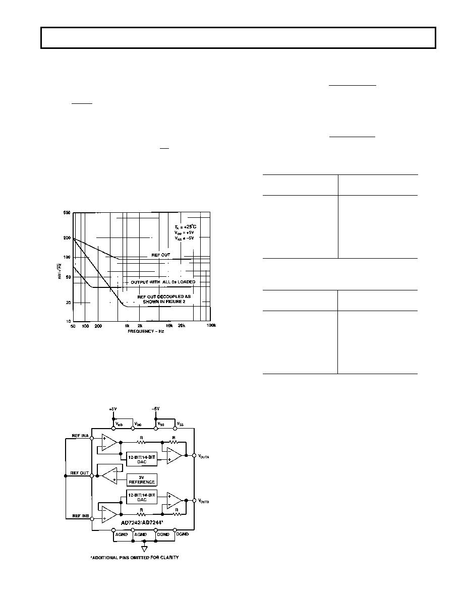
amplifier is typically 1 MHz. The output noise from the
amplifier is low, with a figure of 30 nV/
√Hz at a frequency of
1 kHz. The broadband noise from the amplifier exhibits a
typical peak-to-peak figure of 150
V for a 1 MHz output
bandwidth. Figure 4 shows a typical plot of noise spectral
density versus frequency for the output buffer amplifier and for
the on-chip reference (including and excluding the decoupling
components).
Figure 4. Noise Spectral Density vs. Frequency
TRANSFER FUNCTION
The basic circuit configuration for the AD7242/AD7244 is
shown in Figure 5. Table I and Table II show the ideal input
code to output voltage relationship for the AD7242 and
AD7244 respectively. Input coding for the AD7242/AD7244 is
2s complement.
Figure 5. Basic Connection Diagram
For the AD7242, the output voltage can be expressed in terms
of the input code, N, using the following relationship:
VOUT =
2
N REF IN
4096
where –2048
≤ N ≤ +2047
For the AD7244, the output voltage can be expressed in terms
of the input code, N, using the following relationship:
VOUT =
2
N REF IN
16384
where –8192
≤ N ≤ +8191
Table I. AD7242 Ideal Input/Output Code Table Code
DAC Latch Contents
MSB
LSB
Analog Output, VOUT*
01 11 1111 1111
+2.998535 V
01 11 1111 1110
+2.99707 V
00 00 0000 0001
+0.001465 V
00 00 0000 0000
0 V
11 11 1111 1111
–0.001465 V
10 00 0000 0001
–2.998535 V
10 00 0000 0000
–3 V
*Assuming REF IN = +3 V.
Table II. AD7244 Ideal Input/Output Code Table Code
DAC Latch Contents
MSB
LSB
Analog Output, VOUT*
01 1111 1111 1111
+2.999634 V
01 1111 1111 1110
+2.99268 V
00 0000 0000 0001
+0.000366 V
00 0000 0000 0000
0 V
11 1111 1111 1111
–0.000366 V
10 0000 0000 0001
–2.999634 V
10 0000 0000 0000
–3 V
*Assuming REF IN = +3 V.
OBSOLETE
相关PDF资料 |
PDF描述 |
|---|---|
| AD7244JRZ | 12-/14-Bit DAC, 3 V Buried Zener Reference, DAC |
| AD7245SD | PARALLEL, WORD INPUT LOADING, 12-BIT DAC, CDIP24 |
| AD7249ANZ | LC2MOS Dual 12-Bit Serial DACPORT |
| AD7249ARZ | LC2MOS Dual 12-Bit Serial DACPORT |
| AD7249BRZ | LC2MOS Dual 12-Bit Serial DACPORT |
相关代理商/技术参数 |
参数描述 |
|---|---|
| AD7244JR | 功能描述:IC DAC 14BIT LC2MOS DUAL 28SOIC RoHS:否 类别:集成电路 (IC) >> 数据采集 - 数模转换器 系列:- 产品培训模块:Lead (SnPb) Finish for COTS Obsolescence Mitigation Program 标准包装:1,000 系列:- 设置时间:1µs 位数:8 数据接口:串行 转换器数目:8 电压电源:双 ± 功率耗散(最大):941mW 工作温度:0°C ~ 70°C 安装类型:表面贴装 封装/外壳:24-SOIC(0.295",7.50mm 宽) 供应商设备封装:24-SOIC W 包装:带卷 (TR) 输出数目和类型:8 电压,单极 采样率(每秒):* |
| AD7244JR-REEL | 制造商:Rochester Electronics LLC 功能描述:- Tape and Reel |
| AD7244JRZ | 功能描述:IC DAC 14BIT LC2MOS DUAL 28SOIC RoHS:是 类别:集成电路 (IC) >> 数据采集 - 数模转换器 系列:- 标准包装:1 系列:- 设置时间:4.5µs 位数:12 数据接口:串行,SPI? 转换器数目:1 电压电源:单电源 功率耗散(最大):- 工作温度:-40°C ~ 125°C 安装类型:表面贴装 封装/外壳:8-SOIC(0.154",3.90mm 宽) 供应商设备封装:8-SOICN 包装:剪切带 (CT) 输出数目和类型:1 电压,单极;1 电压,双极 采样率(每秒):* 其它名称:MCP4921T-E/SNCTMCP4921T-E/SNRCTMCP4921T-E/SNRCT-ND |
| AD7244JRZ | 制造商:Analog Devices 功能描述:D/A Converter (D-A) IC |
| AD7244JRZ-REEL | 功能描述:IC DAC 14BIT LC2MOS DUAL 28SOIC RoHS:是 类别:集成电路 (IC) >> 数据采集 - 数模转换器 系列:- 产品培训模块:Data Converter Fundamentals DAC Architectures 标准包装:750 系列:- 设置时间:7µs 位数:16 数据接口:并联 转换器数目:1 电压电源:双 ± 功率耗散(最大):100mW 工作温度:0°C ~ 70°C 安装类型:表面贴装 封装/外壳:28-LCC(J 形引线) 供应商设备封装:28-PLCC(11.51x11.51) 包装:带卷 (TR) 输出数目和类型:1 电压,单极;1 电压,双极 采样率(每秒):143k |
发布紧急采购,3分钟左右您将得到回复。