参数资料
| 型号: | AD7244JR |
| 厂商: | Analog Devices Inc |
| 文件页数: | 11/12页 |
| 文件大小: | 0K |
| 描述: | IC DAC 14BIT LC2MOS DUAL 28SOIC |
| 产品培训模块: | Data Converter Fundamentals DAC Architectures |
| 标准包装: | 1 |
| 设置时间: | 4µs |
| 位数: | 14 |
| 数据接口: | 串行 |
| 转换器数目: | 2 |
| 电压电源: | 双 ± |
| 功率耗散(最大): | 195mW |
| 工作温度: | -40°C ~ 85°C |
| 安装类型: | 表面贴装 |
| 封装/外壳: | 28-SOIC(0.295",7.50mm 宽) |
| 供应商设备封装: | 28-SOIC W |
| 包装: | 管件 |
| 输出数目和类型: | 2 电压,双极 |
| 采样率(每秒): | 250k |
AD7242/AD7244
REV. A
–8–
TIMING AND CONTROL
Communication with the AD7242/AD7244 is via six serial logic
inputs. These consist of separate serial clocks, word framing and
data lines for each DAC. DAC updating is controlled by two
digital inputs: LDACA for updating VOUTA and LDACB for
updating VOUTB. These inputs can be asserted independently of
the microprocessor by an external timer when precise updating
intervals are required. Alternatively, the LDACA and LDACB
inputs can be driven from a decoded address bus allowing the
microprocessor control over DAC updating as well as data
communication to the AD7242/AD7244 input latches.
The AD7242/AD7244 contains two latches per DAC, an input
latch and a DAC latch. Data must be loaded to the input latch
under the control of TCLKA, TFSA and DTA for input Latch
A and TCLKB, TFSB and DTB for input Latch B. Data is then
transferred from input Latch A to DAC Latch A under the control
of the LDACA signal, while LDACB controls the loading of DAC
Latch B from input Latch B. Only the data held in the DAC
latches determines the analog outputs of the AD7242/AD7244.
Data is loaded to the input latches under control of the respec-
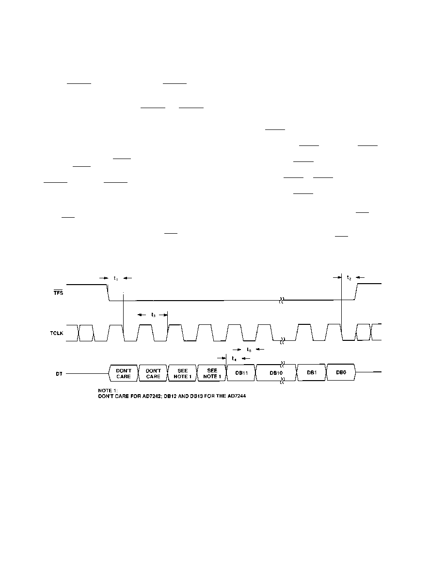
tive TCLK, TFS and DT signals. The AD7242/AD7244
expects a 16-bit stream of serial data on its DT inputs. Data
must be valid on the falling edge of TCLK. The TFS input
provides the frame synchronization signal that tells the AD7242/
AD7244 that valid serial data will be available on the DT input
for the next 16 falling edges of TCLK. Figure 6 shows the
timing diagram for operation of either of the two serial input
ports on the part.
Although 16 bits of data are clocked into the input latch, only
12 bits are transferred into the DAC latch for the AD7242 and
14 bits are transferred for the AD7244. Therefore, 4 bits in the
AD7242 data stream and 2 bits in the AD7244 data stream are
don’t cares since their value does not affect the DAC latch data.
The bit positions are the don’t cares followed by the DAC data
starting with the MSB (see Figure 6).
The respective LDAC signals control the transfer of data to the
respective DAC latches. Normally, data is loaded to the DAC
latch on the falling edge of LDAC. However, if LDAC is held
low, serial data is loaded to the DAC latch on the sixteenth
falling edge of TCLK. If LDAC goes low during the loading of
serial data to the input latch, no DAC latch update takes place
on the falling edge of LDAC. If LDAC stays low until the serial
transfer is completed, then the update takes place on the sixteenth
falling edge of TCLK. If LDAC returns high before the serial
data transfer is completed, no DAC latch update takes place.
If seventeen or more TCLK edges occur while TFS is low, the
seventeenth (and beyond) clock edges are ignored, i.e., no
further data is clocked into the input latch after the sixteenth
TCLK edge following a falling edge on TFS.
Figure 6. AD7242/AD7244 Timing Diagram
相关PDF资料 |
PDF描述 |
|---|---|
| LTC2704CGW-16#PBF | IC DAC 16BIT QUAD VOUT 44-SSOP |
| LTC2704IGW-14#PBF | IC DAC 14BIT QUAD VOUT 44-SSOP |
| AD669BNZ | IC DAC 16BIT MONO W/VREF 28-DIP |
| AD7237AQ | IC DAC 12BIT W/AMP W/BUFF 24CDIP |
| VI-26T-IV | CONVERTER MOD DC/DC 6.5V 150W |
相关代理商/技术参数 |
参数描述 |
|---|---|
| AD7244JR-REEL | 制造商:Rochester Electronics LLC 功能描述:- Tape and Reel |
| AD7244JRZ | 功能描述:IC DAC 14BIT LC2MOS DUAL 28SOIC RoHS:是 类别:集成电路 (IC) >> 数据采集 - 数模转换器 系列:- 标准包装:1 系列:- 设置时间:4.5µs 位数:12 数据接口:串行,SPI? 转换器数目:1 电压电源:单电源 功率耗散(最大):- 工作温度:-40°C ~ 125°C 安装类型:表面贴装 封装/外壳:8-SOIC(0.154",3.90mm 宽) 供应商设备封装:8-SOICN 包装:剪切带 (CT) 输出数目和类型:1 电压,单极;1 电压,双极 采样率(每秒):* 其它名称:MCP4921T-E/SNCTMCP4921T-E/SNRCTMCP4921T-E/SNRCT-ND |
| AD7244JRZ | 制造商:Analog Devices 功能描述:D/A Converter (D-A) IC |
| AD7244JRZ-REEL | 功能描述:IC DAC 14BIT LC2MOS DUAL 28SOIC RoHS:是 类别:集成电路 (IC) >> 数据采集 - 数模转换器 系列:- 产品培训模块:Data Converter Fundamentals DAC Architectures 标准包装:750 系列:- 设置时间:7µs 位数:16 数据接口:并联 转换器数目:1 电压电源:双 ± 功率耗散(最大):100mW 工作温度:0°C ~ 70°C 安装类型:表面贴装 封装/外壳:28-LCC(J 形引线) 供应商设备封装:28-PLCC(11.51x11.51) 包装:带卷 (TR) 输出数目和类型:1 电压,单极;1 电压,双极 采样率(每秒):143k |
| AD7244SQ/883B | 制造商:未知厂家 制造商全称:未知厂家 功能描述:14-Bit Digital-to-Analog Converter |
发布紧急采购,3分钟左右您将得到回复。