参数资料
| 型号: | AD7248ABNZ |
| 厂商: | Analog Devices Inc |
| 文件页数: | 2/16页 |
| 文件大小: | 0K |
| 描述: | IC DAC 12BIT W/REF 24DIP |
| 产品培训模块: | Data Converter Fundamentals DAC Architectures |
| 标准包装: | 18 |
| 系列: | DACPORT® |
| 设置时间: | 7µs |
| 位数: | 12 |
| 数据接口: | 并联 |
| 转换器数目: | 1 |
| 电压电源: | 双 ± |
| 功率耗散(最大): | 210mW |
| 工作温度: | -40°C ~ 85°C |
| 安装类型: | 通孔 |
| 封装/外壳: | 24-DIP(0.300",7.62mm) |
| 供应商设备封装: | 24-PDIP |
| 包装: | 管件 |
| 输出数目和类型: | 1 电压,单极;1 电压,双极 |
| 采样率(每秒): | 142k |
AD7245A/AD7248A
REV. B
–10–
APPLYING THE AD7245A/AD7248A
The internal scaling resistors provided on the AD7245A/
AD7248A allow several output voltage ranges. The part can
produce unipolar output ranges of 0 V to 5 V or 0 V to 10 V
and a bipolar output range of –5 V to +5 V. Connections for
the various ranges are outlined below.
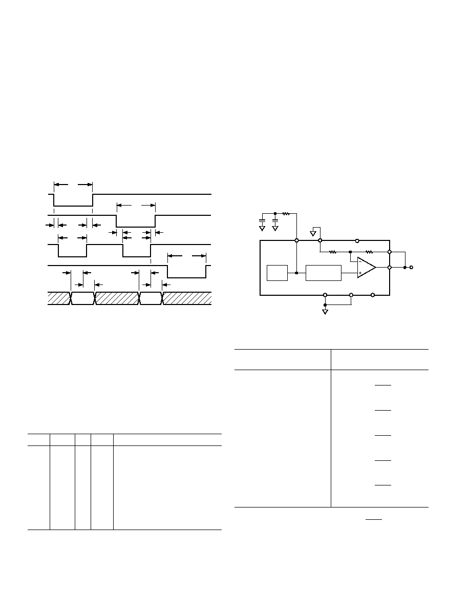
UNIPOLAR (0 V TO 10 V) CONFIGURATION
The first of the configurations provides an output voltage range
of 0 V to 10 V. This is achieved by connecting the bipolar offset
resistor, ROFS, to AGND and connecting RFB to VOUT. In this
configuration the AD7245A/AD7248A can be operated single
supply (VSS = 0 V = AGND). If dual supply performance is
required, a VSS of –12 V to –15 V should be applied. Figure 8
shows the connection diagram for unipolar operation while the
table for output voltage versus the digital code in the DAC latch
is shown in Table III.
VREF
2R
AD7245A/AD7248A*
VOUT
RFB
10
REF OUT
ROFS
10 F
AGND
*DIGITAL CIRCUITRY
OMITTED FOR CLARITY
0.1 F
VDD
DGND
2R
DAC
REF
VSS
Figure 8. Unipolar (0 to 10 V) Configuration
Table III. Unipolar Code Table (0 V to 10 V Range)
DAC Latch Contents
MSB
LSB
Analog Output, VOUT
1 1 1 1
+2 VREF
4095
4096
1 0 0 0
0 0 0 0
0 0 0 1
+2 VREF
2049
4096
1 0 0 0
0 0 0 0
+2 VREF
2048
4096
=+V
REF
0 1 1 1
1 1 1 1
+2 VREF
2047
4096
0 0 0 0
0 0 0 1
+2 VREF
1
4096
0 0 0 0
0 V
NOTE:
1 LSB = 2
VREF(2
–12) = V
REF
1
2048
The
LDAC input controls the transfer of 12-bit data from the
input latch to the DAC latch. This
LDAC signal is also level
triggered, and data is latched into the DAC latch on the rising
edge of
LDAC. The LDAC input is asynchronous and indepen-
dent of
WR. This is useful in many applications especially in
the simultaneous updating of multiple AD7248A outputs. How-
ever, in systems where the asynchronous LDAC can occur during
a write cycle (or vice versa) care must be taken to ensure that
incorrect data is not latched through to the output. In other words,
if LDAC goes low while WR and either CS input are low (or
WR and either CS go low while LDAC is low), then the LDAC
signal must stay low for t7 or longer after WR returns high to
ensure correct data is latched through to the output. The write
cycle timing diagram for the AD7248A is shown in Figure 7.
CSLSB
CSMSB
WR
LDAC
DATA
IN
5V
0V
t4
t3
t5
t6
VALID
DATA
VALID
DATA
5V
0V
5V
0V
5V
0V
5V
0V
t4
t7
t2
t1
t2
t1
Figure 7. AD7248A Write Cycle Timing Diagram
An alternate scheme for writing data to the AD7248A is to tie
the
CSMSB and LDAC inputs together. In this case exercising
CSLSB and WR latches the lower 8 bits into the input latch.
The second write, which exercises
CSMSB, WR and LDAC
loads the upper 4-bit nibble to the input latch and at the same
time transfers the 12-bit data to the DAC latch. This automatic
transfer mode updates the output of the AD7248A in two write
operations. This scheme works equally well for
CSLSB and
LDAC tied together provided the upper 4-bit nibble is loaded
to the input latch followed by a write to the lower 8 bits of
the input latch.
Table II. AD7248A Truth Table
CSLSB CSMSB WR LDAC Function
L
H
L
H
Load LS Byte into Input Latch
LH
g
H
Latches LS Byte into Input Latch
g
H
L
H
Latches LS Byte into Input Latch
H
L
H
Loads MS Nibble into Input Latch
HL
g
H
Latches MS Nibble into Input Latch
H
g
L
H
Latches MS Nibble into Input Latch
H
L
Loads Input Latch into DAC Latch
HH
H
g
Latches Input Latch into DAC Latch
H
L
Loads MS Nibble into Input Latch and
Loads Input Latch into DAC Latch
H
No Data Transfer Operation
H = High State, L = Low State
相关PDF资料 |
PDF描述 |
|---|---|
| AD7538JN | IC DAC 14BIT W/BUFF 24-DIP |
| AD812ANZ | IC OPAMP DUAL CURR-FDBK 8-DIP |
| AD812ARZ | IC OPAMP DUAL CURR-FDBK 8-SOIC |
| AD810ARZ | IC CURR-FDBK AMP VIDEO LP 8-SOIC |
| AD830ARZ | IC VIDEO DIFF AMP HS 8-SOIC |
相关代理商/技术参数 |
参数描述 |
|---|---|
| AD7248ABR | 制造商:Analog Devices 功能描述:DAC 1-CH R-2R 12-bit 20-Pin SOIC W 制造商:Rochester Electronics LLC 功能描述:12-BIT DACPORT (8+4) IC - Bulk |
| AD7248ABR-REEL | 制造商:Rochester Electronics LLC 功能描述:- Tape and Reel |
| AD7248ABRZ | 功能描述:IC DAC 12BIT W/REF 20-SOIC RoHS:是 类别:集成电路 (IC) >> 数据采集 - 数模转换器 系列:DACPORT® 产品培训模块:Data Converter Fundamentals DAC Architectures 标准包装:750 系列:- 设置时间:7µs 位数:16 数据接口:并联 转换器数目:1 电压电源:双 ± 功率耗散(最大):100mW 工作温度:0°C ~ 70°C 安装类型:表面贴装 封装/外壳:28-LCC(J 形引线) 供应商设备封装:28-PLCC(11.51x11.51) 包装:带卷 (TR) 输出数目和类型:1 电压,单极;1 电压,双极 采样率(每秒):143k |
| AD7248ABRZ-REEL | 功能描述:IC DAC 12BIT W/REF 20-SOIC RoHS:是 类别:集成电路 (IC) >> 数据采集 - 数模转换器 系列:DACPORT® 产品培训模块:Data Converter Fundamentals DAC Architectures 标准包装:750 系列:- 设置时间:7µs 位数:16 数据接口:并联 转换器数目:1 电压电源:双 ± 功率耗散(最大):100mW 工作温度:0°C ~ 70°C 安装类型:表面贴装 封装/外壳:28-LCC(J 形引线) 供应商设备封装:28-PLCC(11.51x11.51) 包装:带卷 (TR) 输出数目和类型:1 电压,单极;1 电压,双极 采样率(每秒):143k |
| AD7248AQ | 功能描述:IC DAC 12BIT W/REF 24-CDIP RoHS:否 类别:集成电路 (IC) >> 数据采集 - 数模转换器 系列:DACPORT® 产品培训模块:Data Converter Fundamentals DAC Architectures 标准包装:750 系列:- 设置时间:7µs 位数:16 数据接口:并联 转换器数目:1 电压电源:双 ± 功率耗散(最大):100mW 工作温度:0°C ~ 70°C 安装类型:表面贴装 封装/外壳:28-LCC(J 形引线) 供应商设备封装:28-PLCC(11.51x11.51) 包装:带卷 (TR) 输出数目和类型:1 电压,单极;1 电压,双极 采样率(每秒):143k |
发布紧急采购,3分钟左右您将得到回复。