- 您现在的位置:买卖IC网 > PDF目录165342 > AD7249ANZ (ANALOG DEVICES INC) LC2MOS Dual 12-Bit Serial DACPORT PDF资料下载
参数资料
| 型号: | AD7249ANZ |
| 厂商: | ANALOG DEVICES INC |
| 元件分类: | DAC |
| 英文描述: | LC2MOS Dual 12-Bit Serial DACPORT |
| 中文描述: | DUAL, SERIAL INPUT LOADING, 5 us SETTLING TIME, 12-BIT DAC, PDIP16 |
| 封装: | PLASTIC, DIP-16 |
| 文件页数: | 3/12页 |
| 文件大小: | 149K |
| 代理商: | AD7249ANZ |
AD7249
REV. C
–11–
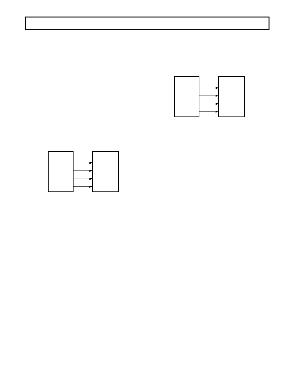
AD7249–68HC11 Interface
Figure 14 shows a serial interface between the AD7249 and the
68HC11 microcontroller. SCK of the 68HC11 drives SCLK of
the AD7249 while the MOSI output drives the serial data line
of the AD7249. The
SYNC signal is derived from a port line
(PC0 shown).
For correct operation of this interface, the 68HC11 should be
configured such that its CPOL bit is a 0 and its CPHA bit is a
1. When data is to be transmitted to the part, PC0 is taken low.
When the 68HC11 is configured like this, data on MOSI is
valid on the falling edge of SCK. The 68HC11 transmits its
serial data in 8-bit bytes with only eight falling clock edges
occurring in the transmit cycle. To load data to the AD7249,
PC0 is left low after the first eight bits are transferred and a sec-
ond byte of data is then transferred serially to the AD7249.
When the second serial transfer is complete, the PC0 line is
taken high.
Figure 14 shows the
LDAC input of the AD7249 being driven
from another bit programmable port line (PC1). As a result,
both DACs can be updated simultaneously by taking
LDAC
low after both DACs latches have updated.
AD7249*
68HC11*
LDAC
SCLK
SDIN
SYNC
PC0
SCK
MOSI
*ADDITIONAL PINS OMITTED FOR CLARITY.
PC1
Figure 14. AD7249–68HC11 Interface
AD7249–87C51 Interface
A serial interface between the AD7249 and the 87C51 micro-
controller is shown in Figure 15. TXD of the 87C51 drives
SCLK of the AD7249 while RXD drives the serial data line of
the part. The
SYNC signal is derived from the port line P3.3
and the
LDAC line is driven port line P3.2.
The 87C51 provides the LSB of its SBUF register as the first
bit in the serial data stream. Therefore, the user will have to
ensure that the data in the SBUF register is arranged correctly
so that the don’t care bits are the first to be transmitted to the
AD7249 and the last bit to be sent is the LSB of the word to be
loaded to the AD7249. When data is to be transmitted to the
part, P3.3 is taken low. Data on RXD is valid on the falling
edge of TXD. The 87C51 transmits its serial data in 8-bit bytes
with only eight falling clock edges occurring in the transmit
cycle. To load data to the AD7249, P3.3 is left low after the
first eight bits are transferred, and a second byte of data is then
transferred serially to the AD7249 with DB12 used to select
the appropriate DAC register. When the second serial transfer
is complete, the P3.3 line is taken high and then taken low
again to start the loading sequence to the second DAC (see
timing diagram Figure 8).
Figure 15 shows the
LDAC input of the AD7249 driven from
the bit programmable port line P3.2. As a result, both DAC
outputs can be updated simultaneously by taking the
LDAC
line low following the completion of the write cycle to the sec-
ond DAC. Alternatively
LDAC could be hardwired low and the
analog output will be updated on the sixteenth falling edge of
TXD after the
SYNC signal for the DAC has gone low.
AD7249*
87C51*
LDAC
SCLK
SDIN
SYNC
P3.3
TXD
RXD
*ADDITIONAL PINS OMITTED FOR CLARITY.
P3.2
Figure 15. AD7249–87C51 Interface
APPLICATIONS
OPTO-ISOLATED INTERFACE
In many process control type applications it is necessary to
provide an isolation barrier between the controller and the
unit being controlled. Opto-isolators can provide voltage
isolation in excess of 3 k
. The serial loading structure of the
AD7249 makes it ideal for opto-isolated interfaces as the num-
ber of interface lines is kept to a minimum.
Figure 16 shows a 2-channel isolated interface using the
AD7249.
The sequence of events to program the output channels is as
follows.
1. Take the
SYNC line low.
2. Transmit the 16-bit word for DAC A (DB 12 of the 16-bit
data word selects the DAC, DB12 = 0 to select DAC A) and
bring the
SYNC line high after the 16 bits have been trans-
mitted.
3. Bring
SYNC line low again and transmit 16 bits for DAC B,
bring
SYNC back high at end of transmission.
4. Pulse the
LDAC line low. This updates both output chan-
nels simultaneously on the falling edge of
LDAC.
相关PDF资料 |
PDF描述 |
|---|---|
| AD7249ARZ | LC2MOS Dual 12-Bit Serial DACPORT |
| AD7249BRZ | LC2MOS Dual 12-Bit Serial DACPORT |
| AD7302BNZ | 2.7 V to 5.5 V, Parallel Input Dual Voltage Output 8-Bit DAC |
| AD7302BR-REEL7 | 2.7 V to 5.5 V, Parallel Input Dual Voltage Output 8-Bit DAC |
| AD7302BRUZ | 2.7 V to 5.5 V, Parallel Input Dual Voltage Output 8-Bit DAC |
相关代理商/技术参数 |
参数描述 |
|---|---|
| AD7249ANZ | 制造商:Analog Devices 功能描述:IC 12-BIT DAC |
| AD7249AR | 功能描述:IC DAC 12BIT SRL W/REF 16-SOIC RoHS:否 类别:集成电路 (IC) >> 数据采集 - 数模转换器 系列:DACPORT® 产品培训模块:Data Converter Fundamentals DAC Architectures 标准包装:750 系列:- 设置时间:7µs 位数:16 数据接口:并联 转换器数目:1 电压电源:双 ± 功率耗散(最大):100mW 工作温度:0°C ~ 70°C 安装类型:表面贴装 封装/外壳:28-LCC(J 形引线) 供应商设备封装:28-PLCC(11.51x11.51) 包装:带卷 (TR) 输出数目和类型:1 电压,单极;1 电压,双极 采样率(每秒):143k |
| AD7249AR-REEL | 功能描述:数模转换器- DAC LC2MOS DUAL 12-BIT SERIAL IC RoHS:否 制造商:Analog Devices 转换器数量:4 DAC 输出端数量:4 转换速率: 分辨率:12 bit 接口类型:Serial (I2C) 稳定时间: 最大工作温度:+ 105 C 安装风格: 封装 / 箱体:TSSOP 封装:Reel |
| AD7249ARZ | 功能描述:IC DAC 12BIT SRL W/REF 16-SOIC RoHS:是 类别:集成电路 (IC) >> 数据采集 - 数模转换器 系列:DACPORT® 产品培训模块:Lead (SnPb) Finish for COTS Obsolescence Mitigation Program 标准包装:50 系列:- 设置时间:4µs 位数:12 数据接口:串行 转换器数目:2 电压电源:单电源 功率耗散(最大):- 工作温度:-40°C ~ 85°C 安装类型:表面贴装 封装/外壳:8-TSSOP,8-MSOP(0.118",3.00mm 宽) 供应商设备封装:8-uMAX 包装:管件 输出数目和类型:2 电压,单极 采样率(每秒):* 产品目录页面:1398 (CN2011-ZH PDF) |
| AD7249ARZ | 制造商:Analog Devices 功能描述:IC 12-BIT DAC |
发布紧急采购,3分钟左右您将得到回复。