参数资料
| 型号: | AD7249BNZ |
| 厂商: | Analog Devices Inc |
| 文件页数: | 9/14页 |
| 文件大小: | 0K |
| 描述: | IC DAC 12BIT SRL W/REF 16DIP |
| 产品培训模块: | Data Converter Fundamentals DAC Architectures |
| 标准包装: | 25 |
| 系列: | DACPORT® |
| 设置时间: | 10µs |
| 位数: | 12 |
| 数据接口: | 串行 |
| 转换器数目: | 2 |
| 电压电源: | 双 ± |
| 功率耗散(最大): | 300mW |
| 工作温度: | -40°C ~ 85°C |
| 安装类型: | 通孔 |
| 封装/外壳: | 16-DIP(0.300",7.62mm) |
| 供应商设备封装: | 16-PDIP |
| 包装: | 管件 |
| 输出数目和类型: | 2 电压,单极;2 电压,双极 |
| 采样率(每秒): | 125k |
–4–
AD7249
PIN FUNCTION DESCRIPTION (DIP & SOIC PIN NUMBERS)
Pin
Mnemonic
Description
11
REFOUT
Voltage Reference Output. The internal 5 V analog reference is provided at this pin. To operate the
part using its internal reference, REFOUT should be connected to REFIN.
12
REFIN
Voltage Reference Input. It is internally buffered before being applied to both DACs. The nominal
reference voltage for specified operation of the AD7249 is 5 V.
13ROFSB
Output Offset Resistor for the amplifier of DAC B. It is connected to VOUTB for the +5 V range, to
AGND for the +10 V range and to REFIN for the –5 V to +5 V range.
14VOUTB
Analog Output Voltage of DAC B. This is the buffer amplifier output voltage. Three different output
voltage ranges can be chosen: 0 V to +5 V, 0 V to +10 V and –5 V to +5 V.
15
AGND
Analog Ground. Ground reference for all analog circuitry.
16
CLR
Clear, Logic Input. Taking this input low clears both DACs. It sets VOUTA and VOUTB to 0 V in both
unipolar ranges and the twos complement bipolar range and to –REFIN in the offset binary bipolar
range.
17
BIN/COMP
Logic Input. This input selects the data format to be either binary or twos complement. In both uni-
polar ranges natural binary format is selected by connecting this input to a Logic “0”. In the bipolar
configuration offset binary format is selected with a Logic “0” while a Logic “1” selects twos complement.
18
DGND
Digital Ground. Ground reference for all digital circuitry.
19
SDIN
Serial Data In, Logic Input. The 16-bit serial data word is applied to this input.
10
LDAC
Load DAC, Logic Input. Updates both DAC outputs. The DAC outputs are updated on the falling
edge of this signal or alternatively if this line is permanently low, an automatic update mode is se-
lected whereby both DACs are updated on the 16th falling SCLK pulse.
11
SCLK
Serial Clock, Logic Input. Data is clocked into the input register on each falling SCLK edge.
12
SYNC
Data Synchronization Pulse, Logic Input. Taking this input low initializes the internal logic in readi-
ness for a new data word.
13
VDD
Positive Power Supply.
14
VOUTA
Analog Output Voltage of DAC A. This is the buffer amplifier output voltage. Three different output
voltage ranges can be chosen: 0 V to +5 V, 0 V to +10 V and –5 V to +5 V.
15
VSS
Negative Power Supply (used for the output amplifier only) may be connected to 0 V for single sup-
ply operation or –12 V to –15 V for dual supplies.
16
ROFSA
Output Offset Resistor for the amplifier of DAC A. It is connected to VOUTA for the +5 V range, to
AGND for the +10 V range and to REFIN for the –5 V to +5 V range.
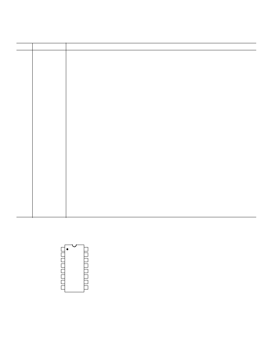
PIN CONFIGURATIONS
(DIP and SOIC)
TOP VIEW
(Not to Scale)
16
15
14
13
12
11
10
9
1
2
3
4
5
6
7
8
REFOUT
ROFSA
AD7249
REFIN
VSS
ROFSB
VOUTA
VOUTB
VDD
AGND
SYNC
CLR
SCLK
BIN/COMP
LDAC
DGND
SDIN
REV. D
相关PDF资料 |
PDF描述 |
|---|---|
| AD818ANZ | IC VIDEO OPAMP 130MHZ LP 8-DIP |
| AD420AR-32 | IC DAC SRL 16BIT 24-SOIC |
| LT6553CGN#PBF | IC AMP TRPL VIDEO GAIN2 16-SSOP |
| AD660ARZ-REEL | IC DAC 16BIT MONO W/VREF 24-SOIC |
| AD817AN | IC OPAMP HS LP 8-DIP |
相关代理商/技术参数 |
参数描述 |
|---|---|
| AD7249BR | 功能描述:IC DAC 12BIT SRL W/REF 16-SOIC RoHS:否 类别:集成电路 (IC) >> 数据采集 - 数模转换器 系列:DACPORT® 产品培训模块:Data Converter Fundamentals DAC Architectures 标准包装:750 系列:- 设置时间:7µs 位数:16 数据接口:并联 转换器数目:1 电压电源:双 ± 功率耗散(最大):100mW 工作温度:0°C ~ 70°C 安装类型:表面贴装 封装/外壳:28-LCC(J 形引线) 供应商设备封装:28-PLCC(11.51x11.51) 包装:带卷 (TR) 输出数目和类型:1 电压,单极;1 电压,双极 采样率(每秒):143k |
| AD7249BR-REEL | 功能描述:IC DAC 12BIT SRL W/REF 16-SOIC RoHS:否 类别:集成电路 (IC) >> 数据采集 - 数模转换器 系列:DACPORT® 产品培训模块:Data Converter Fundamentals DAC Architectures 标准包装:750 系列:- 设置时间:7µs 位数:16 数据接口:并联 转换器数目:1 电压电源:双 ± 功率耗散(最大):100mW 工作温度:0°C ~ 70°C 安装类型:表面贴装 封装/外壳:28-LCC(J 形引线) 供应商设备封装:28-PLCC(11.51x11.51) 包装:带卷 (TR) 输出数目和类型:1 电压,单极;1 电压,双极 采样率(每秒):143k |
| AD7249BRZ | 功能描述:IC DAC 12BIT SRL W/REF 16SOIC RoHS:是 类别:集成电路 (IC) >> 数据采集 - 数模转换器 系列:DACPORT® 标准包装:1 系列:- 设置时间:4.5µs 位数:12 数据接口:串行,SPI? 转换器数目:1 电压电源:单电源 功率耗散(最大):- 工作温度:-40°C ~ 125°C 安装类型:表面贴装 封装/外壳:8-SOIC(0.154",3.90mm 宽) 供应商设备封装:8-SOICN 包装:剪切带 (CT) 输出数目和类型:1 电压,单极;1 电压,双极 采样率(每秒):* 其它名称:MCP4921T-E/SNCTMCP4921T-E/SNRCTMCP4921T-E/SNRCT-ND |
| AD7249BRZ-REEL | 功能描述:IC DAC 12BIT SRL W/REF 16SOIC RoHS:是 类别:集成电路 (IC) >> 数据采集 - 数模转换器 系列:DACPORT® 产品培训模块:Data Converter Fundamentals DAC Architectures 标准包装:750 系列:- 设置时间:7µs 位数:16 数据接口:并联 转换器数目:1 电压电源:双 ± 功率耗散(最大):100mW 工作温度:0°C ~ 70°C 安装类型:表面贴装 封装/外壳:28-LCC(J 形引线) 供应商设备封装:28-PLCC(11.51x11.51) 包装:带卷 (TR) 输出数目和类型:1 电压,单极;1 电压,双极 采样率(每秒):143k |
| AD7249SQ | 功能描述:数模转换器- DAC LC2MOS DUAL 12-BIT SERIAL IC RoHS:否 制造商:Analog Devices 转换器数量:4 DAC 输出端数量:4 转换速率: 分辨率:12 bit 接口类型:Serial (I2C) 稳定时间: 最大工作温度:+ 105 C 安装风格: 封装 / 箱体:TSSOP 封装:Reel |
发布紧急采购,3分钟左右您将得到回复。