参数资料
| 型号: | AD7249BR |
| 厂商: | Analog Devices Inc |
| 文件页数: | 2/14页 |
| 文件大小: | 0K |
| 描述: | IC DAC 12BIT SRL W/REF 16-SOIC |
| 产品培训模块: | Data Converter Fundamentals DAC Architectures |
| 标准包装: | 1 |
| 系列: | DACPORT® |
| 设置时间: | 10µs |
| 位数: | 12 |
| 数据接口: | 串行 |
| 转换器数目: | 2 |
| 电压电源: | 双 ± |
| 功率耗散(最大): | 300mW |
| 工作温度: | -40°C ~ 85°C |
| 安装类型: | 表面贴装 |
| 封装/外壳: | 16-SOIC(0.295",7.50mm 宽) |
| 供应商设备封装: | 16-SOIC W |
| 包装: | 管件 |
| 输出数目和类型: | 2 电压,单极;2 电压,双极 |
| 采样率(每秒): | 125k |
–10–
AD7249
MICROPROCESSOR INTERFACING
Microprocessor interfacing to the AD7249 is via a serial bus
which uses standard protocol compatible with DSP processors
and microcontrollers. The communications channel requires a
three-wire interface consisting of a clock signal, a data signal
and a synchronization signal. The AD7249 requires a 16-bit
data word with data valid on the falling edge of SCLK. For all
the interfaces, the DAC update may be done automatically
when all the data is clocked in or it may be done under control
of
LDAC.
Figures 11 to 15 show the AD7249 configured for interfacing to
a number of popular DSP processors and microcontrollers.
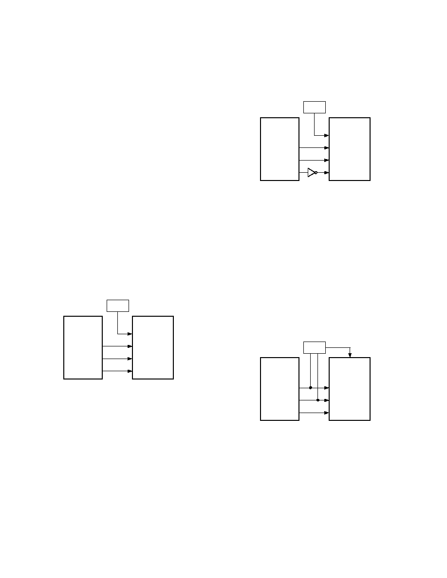
AD7249–ADSP-2101/ADSP-2102 Interface
Figure 11 shows a serial interface between the AD7249 and the
ADSP-2101/ADSP-2102 DSP processor. The ADSP-2101/
ADSP-2102 contains two serial ports and either port may be
used in the interface. The data transfer is initiated by
TFS
going low. Data from the ADSP-2101/ADSP-2102 is clocked
into the AD7249 on the falling edge of SCLK. DB12 of the
16-bit serial data stream selects the DAC to be updated. Both
DACs can be updated by holding
LDAC high while performing
two write cycles to the DAC.
TFS must be taken high after
each 16 bit write cycle.
LDAC is brought low at the end of the
second cycle and both DAC outputs are updated together. In
the interface shown the DAC is updated using an external timer
which generates an
LDAC pulse. This could also be done using
a control or decoded address line from the processor. Alterna-
tively, if the
LDAC input is hardwired low the output update
takes place automatically on the 16th falling edge of SCLK.
AD7249*
ADSP-2101/
ADSP-2102*
LDAC
SCLK
SDIN
SYNC
SCLK
DT
TFS
TIMER
*ADDITIONAL PINS OMITTED FOR CLARITY.
Figure 11. AD7249–ADSP-2101/ADSP-2102 Interface
AD7249–DSP56000 Interface
A serial interface between the AD7249 and the DSP56000 is
shown in Figure 12. The DSP56000 is configured for Normal
Mode Asynchronous operation with Gated Clock. It is also set
up for a 16-bit word with SCK and SC2 as outputs and the
FSL control bit set to a “0.” SCK is internally generated on the
DSP56000 and applied to the AD7249 SCLK input. Data from
the DSP56000 is valid on the falling edge of SCK. The SC2
output provides the framing pulse for valid data. This line must
be inverted before being applied to the
SYNC input of the
AD7249.
AD7249*
DSP56000
LDAC
SCLK
SDIN
SYNC
SCK
STD
SC2
TIMER
*ADDITIONAL PINS OMITTED FOR CLARITY.
Figure 12. AD7249–DSP56000 Interface
In this interface an external
LDAC pulse generated from an
external timer is used to update the outputs of the DACs. This
update can also be produced using a bit programmable control
line from the DSP56000.
AD7249–TMS32020 Interface
Figure 13 shows a serial interface between the AD7249 and the
TMS32020 DSP processor. In this interface, the CLKX and
FSX signals for the TMS32020 should be generated using
external clock/timer circuitry. The FSX pin of the TMS32020
must be configured as an input. Data from the TMS32020 is
valid on the falling edge of CLKX.
The clock/timer circuitry generates the
LDAC signal for the
AD7249 to synchronize the update of the output with the serial
transmission. Alternatively, the automatic update mode may be
selected by connecting
LDAC to DGND.
AD7249*
TMS32020
LDAC
SCLK
SDIN
SYNC
FSX
CLKX
DX
CLOCK/
TIMER
*ADDITIONAL PINS OMITTED FOR CLARITY.
Figure 13. AD7249–TMS32020 Interface
REV. D
相关PDF资料 |
PDF描述 |
|---|---|
| AD7262BSTZ | IC ADC 2CH 12BIT PGA/COM 48LQFP |
| AD7264BCPZ | IC ADC 14BIT 2CH 1MSPS 48LFCSP |
| AD7265BSUZ-REEL7 | IC ADC 12BIT 3CHAN 1MSPS 32TQFP |
| AD7266BSUZ | IC ADC 12BIT 3CH 2MSPS 32-TQFP |
| AD7274BRM | IC ADC 12BIT 3MSPS HS LP 8MSOP |
相关代理商/技术参数 |
参数描述 |
|---|---|
| AD7249BR-REEL | 功能描述:IC DAC 12BIT SRL W/REF 16-SOIC RoHS:否 类别:集成电路 (IC) >> 数据采集 - 数模转换器 系列:DACPORT® 产品培训模块:Data Converter Fundamentals DAC Architectures 标准包装:750 系列:- 设置时间:7µs 位数:16 数据接口:并联 转换器数目:1 电压电源:双 ± 功率耗散(最大):100mW 工作温度:0°C ~ 70°C 安装类型:表面贴装 封装/外壳:28-LCC(J 形引线) 供应商设备封装:28-PLCC(11.51x11.51) 包装:带卷 (TR) 输出数目和类型:1 电压,单极;1 电压,双极 采样率(每秒):143k |
| AD7249BRZ | 功能描述:IC DAC 12BIT SRL W/REF 16SOIC RoHS:是 类别:集成电路 (IC) >> 数据采集 - 数模转换器 系列:DACPORT® 标准包装:1 系列:- 设置时间:4.5µs 位数:12 数据接口:串行,SPI? 转换器数目:1 电压电源:单电源 功率耗散(最大):- 工作温度:-40°C ~ 125°C 安装类型:表面贴装 封装/外壳:8-SOIC(0.154",3.90mm 宽) 供应商设备封装:8-SOICN 包装:剪切带 (CT) 输出数目和类型:1 电压,单极;1 电压,双极 采样率(每秒):* 其它名称:MCP4921T-E/SNCTMCP4921T-E/SNRCTMCP4921T-E/SNRCT-ND |
| AD7249BRZ-REEL | 功能描述:IC DAC 12BIT SRL W/REF 16SOIC RoHS:是 类别:集成电路 (IC) >> 数据采集 - 数模转换器 系列:DACPORT® 产品培训模块:Data Converter Fundamentals DAC Architectures 标准包装:750 系列:- 设置时间:7µs 位数:16 数据接口:并联 转换器数目:1 电压电源:双 ± 功率耗散(最大):100mW 工作温度:0°C ~ 70°C 安装类型:表面贴装 封装/外壳:28-LCC(J 形引线) 供应商设备封装:28-PLCC(11.51x11.51) 包装:带卷 (TR) 输出数目和类型:1 电压,单极;1 电压,双极 采样率(每秒):143k |
| AD7249SQ | 功能描述:数模转换器- DAC LC2MOS DUAL 12-BIT SERIAL IC RoHS:否 制造商:Analog Devices 转换器数量:4 DAC 输出端数量:4 转换速率: 分辨率:12 bit 接口类型:Serial (I2C) 稳定时间: 最大工作温度:+ 105 C 安装风格: 封装 / 箱体:TSSOP 封装:Reel |
| AD7249SQ/883B | 制造商:未知厂家 制造商全称:未知厂家 功能描述:12-Bit Digital-to-Analog Converter |
发布紧急采购,3分钟左右您将得到回复。