- 您现在的位置:买卖IC网 > PDF目录10967 > AD724JRZ-RL (Analog Devices Inc)IC ENCODER RGB TO NTSC 16SOIC TR PDF资料下载
参数资料
| 型号: | AD724JRZ-RL |
| 厂商: | Analog Devices Inc |
| 文件页数: | 4/15页 |
| 文件大小: | 0K |
| 描述: | IC ENCODER RGB TO NTSC 16SOIC TR |
| 标准包装: | 1,000 |
| 类型: | 视频编码器 |
| 应用: | RGB 至 NTSC/PAL |
| 电压 - 电源,数字: | 4.75 V ~ 5.25 V |
| 安装类型: | 表面贴装 |
| 封装/外壳: | 16-SOIC(0.295",7.50mm 宽) |
| 供应商设备封装: | 16-SOIC W |
| 包装: | 带卷 (TR) |
REV. B
–12–
AD724
With the crystal selection circuit described above, the unse-
lected crystal and diode provide additional shunt capacitance
across the selected crystal. The evaluation board tested actually
required no additional capacitance in order to run at the
proper frequency for each video standard. However, depending
on the layout, some circuits might require a small capacitor
from FIN (Pin 3) to ground to operate with the chrominance
at the proper frequency.
SUBCARRIER FREQUENCY MEASUREMENT
It is extremely difficult to measure the oscillation frequency of
the AD724 when operating with a crystal. The only place where
a CW oscillation is present is at the FIN pin. However, probing
with any type of probe (even a low capacitance FET probe) at
this node will either kill the oscillation or change the frequency
of oscillation, so the unprobed oscillating frequency cannot be
discerned. Neither the composite video nor chroma signals have
the subcarrier represented in a CW fashion. (The LUMA signal
does not contain any of the subcarrier.) This makes it virtually
impossible to accurately measure the subcarrier frequency of
these signals with any oscilloscope technique.
Two methods have been found to accurately measure the sub-
carrier oscillating frequency. The first uses a spectrum analyzer
like the HP3585A that has an accurate frequency counter built
in. By looking at either the COMP or CHROMA output of the
AD724, a spectrum can be observed that displays the tone of
the subcarrier frequency as the largest lobe.
The CHROMA or COMP output of the AD724 should be
input into the spectrum analyzer either by means of a scope
probe into the 1 M
input port or a 75 cable that can be
directly terminated by the 75
input termination selection of
the HP3585A. Each of these signals has present at least the
color burst signal on almost every line, which will be the domi-
nant tone in the frequency band near its nominal frequency.
Sidelobes will be observed on either side of the central lobe
spaced at 50 Hz (PAL) or 60 Hz (NTSC) intervals due to the
vertical scanning rate of the video signals. There will also be
sidelobes on either side at about 15.75 kHz intervals, but these
will not be observable with the span set to only a few kHz.
The center frequency of the spectrum analyzer should be set to
the subcarrier frequency of the standard that is to be observed.
The span should be set to 1 kHz–3 kHz and the resolution
bandwidth (RBW) set to between 10 Hz to 100 Hz. A combina-
tion of wider frequency span and narrower RBW will require a
long time for sweeping the entire range. Increasing the RBW
will speed up the sweep at the expense of widening the “humps”
in the subcarrier tone and the sideband tones.
Once the subcarrier is located, it can be moved to the center of
the display and the span can be narrowed to cover only that range
necessary to see it. The RBW can then be narrowed to produce
an acceptably fast sweep with good resolution.
The marker can now be placed at the location of the subcarrier
tone and the frequency counter turned on. The next scan across
the location of the marker will measure and display the subcarrier
frequency to better than 1 Hz resolution.
A second means for measuring the subcarrier frequency of an
AD724 operating from a crystal involves equipment more spe-
cialized than a spectrum analyzer. The technique requires a
Tektronix VM700A video system measurement instrument.
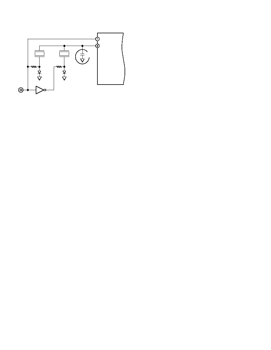
R1
10k
Y1
Y2
CR1
IN4148
CR2
IN4148
STND
AD724
FIN
HC04
U1
OPTIONAL
NOTES: Y1 = 3.579545MHz
Y2 = 4.433620MHz
R2
10k
PAL
NTSC
0-5pF
Figure 17. Crystal Selection Circuit
Pin 1 (STND) of the AD724 is used to program the internal
operation for either NTSC (HIGH) or PAL (LOW). For NTSC
operation in this application the HIGH signal is also used to
drive R1 and the input of inverter U1. This creates a LOW
signal at the output of U1.
The HIGH (+5 V) signal applied to R1 forward biases CR1 with
approximately 450
A of current. This turns the diode “on” (low
impedance with a forward voltage of approximately 0.6 V) and
selects Y1 as the crystal to run the oscillator on the AD724. The
bias across the diode does not affect the operation of the
oscillator.
The LOW (0 V) output of the inverter U1 is applied to R2. This
creates a 0 V bias condition across CR2 because its cathode is
also at ground potential. This diode is now in the “off” (high
impedance) state, because it takes approximately 600 mV of
forward bias to turn a diode “on” to any significant degree. The
“off” condition of the diode does, however, look like a capacitor
of a few pF.
For PAL operation, the STND signal that drives Pin 1 is set LOW
(0 V). This programs the AD724 for PAL operation, deselects the
NTSC crystal (Y1), because CR1 has no bias voltage across it and
selects the PAL crystal (Y2) by forward biasing CR2.
In order to ensure that the circuits described above operate
under the same conditions with either crystal selected, it is im-
portant to use a logic signal from a CMOS type logic family
whose output swings fully from ground to +5 V when operating
on a +5 V supply. Other TTL type logic families don’t swing
this far and might cause problems as a result of variations in the
diode bias voltages between the two different crystal selection
modes.
FREQUENCY TUNING
A parallel resonant crystal, is the type required for the AD724
oscillator, will work at its operating frequency when it has a
specified capacitance in parallel with its terminals. For the
AD724 evaluation board, it was found that approximately 10 pF
was required across either the PAL or NTSC crystal for proper
tuning. The parallel capacitance specified for these crystals is
17 pF for the NTSC crystal and 20 pF for the PAL crystal. The
parasitic capacitance of the PC board, packaging and the internal
circuitry of the AD724 appear to be contributing 7 pF–10 pF in
shunt with the crystal. A direct measurement of this was not
made, but the value is inferred from the measured results.
相关PDF资料 |
PDF描述 |
|---|---|
| VE-B42-IX-B1 | CONVERTER MOD DC/DC 15V 75W |
| VI-B1F-IY-F3 | CONVERTER MOD DC/DC 72V 50W |
| VE-B42-IW-B1 | CONVERTER MOD DC/DC 15V 100W |
| VE-B41-IX-B1 | CONVERTER MOD DC/DC 12V 75W |
| VE-26P-IY-F2 | CONVERTER MOD DC/DC 13.8V 50W |
相关代理商/技术参数 |
参数描述 |
|---|---|
| AD725 | 制造商:AD 制造商全称:Analog Devices 功能描述:Low Cost RGB to NTSC/PAL Encoder with Luma Trap Port |
| AD725AR | 制造商:Analog Devices 功能描述:RGB to NTSC and PAL Encoder 16-Pin SOIC W 制造商:Rochester Electronics LLC 功能描述:SOIC LOW COST VIDEO ENCODER - Bulk 制造商:Analog Devices 功能描述:TUBE / SOIC LOW COST VIDEO ENCODER |
| AD725AR-REEL | 制造商:Analog Devices 功能描述:RGB to NTSC and PAL Encoder 16-Pin SOIC W T/R 制造商:Rochester Electronics LLC 功能描述:SOIC LOW COST VIDEO ENCODER - Tape and Reel |
| AD725AR-REEL7 | 制造商:Analog Devices 功能描述:RGB to NTSC and PAL Encoder 16-Pin SOIC W T/R 制造商:Rochester Electronics LLC 功能描述:SOIC LOW COST VIDEO ENCODER - Tape and Reel |
| AD725ARZ | 功能描述:IC ENCODER RGB TO NTSC 16-SOIC RoHS:是 类别:集成电路 (IC) >> 接口 - 编码器,解码器,转换器 系列:- 产品变化通告:Development Systems Discontinuation 26/Apr/2011 标准包装:1 系列:- 类型:编码器 应用:DVB-S.2 系统 电压 - 电源,模拟:- 电压 - 电源,数字:- 安装类型:- 封装/外壳:模块 供应商设备封装:模块 包装:散装 其它名称:Q4645799 |
发布紧急采购,3分钟左右您将得到回复。