- 您现在的位置:买卖IC网 > PDF目录10254 > AD7264BCPZ-5 (Analog Devices Inc)IC ADC 14BIT 2CH 500KSPS 48LFCSP PDF资料下载
参数资料
| 型号: | AD7264BCPZ-5 |
| 厂商: | Analog Devices Inc |
| 文件页数: | 19/29页 |
| 文件大小: | 0K |
| 描述: | IC ADC 14BIT 2CH 500KSPS 48LFCSP |
| 标准包装: | 1 |
| 位数: | 14 |
| 采样率(每秒): | 500k |
| 数据接口: | DSP,MICROWIRE?,QSPI?,串行,SPI? |
| 转换器数目: | 2 |
| 功率耗散(最大): | 175mW |
| 电压电源: | 单电源 |
| 工作温度: | -40°C ~ 105°C |
| 安装类型: | 表面贴装 |
| 封装/外壳: | 48-VFQFN 裸露焊盘,CSP |
| 供应商设备封装: | 48-LFCSP-VQ(7x7) |
| 包装: | 托盘 |
| 输入数目和类型: | * |
第1页第2页第3页第4页第5页第6页第7页第8页第9页第10页第11页第12页第13页第14页第15页第16页第17页第18页当前第19页第20页第21页第22页第23页第24页第25页第26页第27页第28页第29页
Data Sheet
AD7264
Rev. B | Page 25 of 28
CALIBRATION
INTERNAL OFFSET CALIBRATION
The AD7264 allows the user to calibrate the offset of the device
using the CAL pin. This is achieved by setting the CAL pin to a
high logic level, which initiates a calibration on the next CS
falling edge. The calibration requires one full conversion cycle,
which contains a CS falling edge followed by 19 SCLK cycles.
The CAL pin can remain high for more than one conversion, if
desired, and the AD7264 continues to calibrate.
The CAL pin should be driven high only when the CS pin is
high or after 19 SCLK cycles have elapsed when CS is low, that
is, between conversions. The CAL pin must be driven high t12
before CS goes low. If the CS pin goes low before t12 elapses, the
calibration result will be inaccurate for the current conversion;
if the CAL pin remains high, the subsequent calibration conver-
sion is correct. If the CAL pin is set to a logic high state during a
conversion, that conversion result is corrupted.
If the CAL pin has been held high for a minimum of one
conversion and when t12 and t11 have been adhered to, the
calibration is complete after the 19th SCLK cycle and the CAL
pin can be driven to a logic low state. The next CS falling edge
after the CAL pin has been driven to a low logic state initiates
a conversion of the differential analog input signal for both
ADC A and ADC B.
Alternatively, the control register can be used to initiate an offset
calibration. This is done by setting the CAL bit in the control
register to 1. The calibration is then initiated on the next CS
falling edge, but the current conversion is corrupted. The ADCs
on the AD7264 must remain fully powered up to complete the
internal calibration.
The AD7264 registers store the offset value, which can easily be
accessed by the user (see the Reading from a Register section).
When the device is calibrating, the differential analog inputs
for each respective ADC are shorted together internally and a
conversion is performed. A digital code representing the offset is
stored internally in the offset registers, and subsequent conver-
sion results have this measured offset removed.
When the AD7264 is calibrated, the calibration results stored in
the internal device registers are relevant only for the particular
PGA gain selected at the time of calibration. If the PGA gain is
changed, the AD7264 must be recalibrated. If the device is not
recalibrated when the PGA gain is changed, the offset for the
previous gain setting continues to be removed from the digital
output code, which may lead to inaccuracies.
The offset range that can be calibrated for is ±500 LSB at a gain
of 1. The maximum offset voltage that can be calibrated for is
reduced as the gain of the PGA is increased.
Table 12 details the maximum offset voltage that can be removed
by the AD7264 without compromising the available digital
output code range. The least significant bit size is AVCC/2Bits,
which is 5/16,384 or 305 μV for the AD7264. The maximum
removable offset voltage is given by
Gain
μV
305
LSB
500
×
±
Table 12. Offset Voltage Range
Gain
Maximum Removable Offset Voltage
1
±152.5 mV
2
±76.25 mV
3
±50.83 mV
32
±4.765 mV
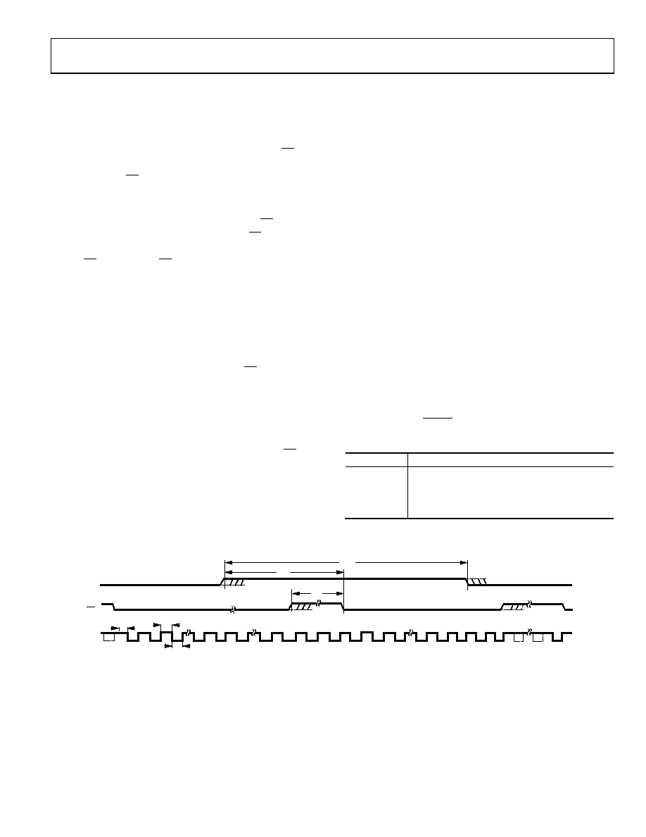
06732-
035
CS
SCLK
CAL
20
1
2
3
21
19
t2
t6
t8
t7
t12
t11
33
32
21
20
19
3
2
1
Figure 36. Calibration Timing Diagram
相关PDF资料 |
PDF描述 |
|---|---|
| VI-23W-CU-F1 | CONVERTER MOD DC/DC 5.5V 200W |
| VE-22T-MX-F2 | CONVERTER MOD DC/DC 6.5V 75W |
| VI-23V-IW-S | CONVERTER MOD DC/DC 5.8V 100W |
| VE-22R-MX-F4 | CONVERTER MOD DC/DC 7.5V 75W |
| AD7450ABRM | IC ADC 12BIT DIFF-IN 1MSPS 8MSOP |
相关代理商/技术参数 |
参数描述 |
|---|---|
| AD7264BCPZ-5-RL7 | 功能描述:IC ADC 14BIT 2CH 500KSPS 48LFCSP RoHS:是 类别:集成电路 (IC) >> 数据采集 - 模数转换器 系列:- 标准包装:1,000 系列:- 位数:16 采样率(每秒):45k 数据接口:串行 转换器数目:2 功率耗散(最大):315mW 电压电源:模拟和数字 工作温度:0°C ~ 70°C 安装类型:表面贴装 封装/外壳:28-SOIC(0.295",7.50mm 宽) 供应商设备封装:28-SOIC W 包装:带卷 (TR) 输入数目和类型:2 个单端,单极 |
| AD7264BCPZ-RL7 | 功能描述:IC ADC 14BIT 2CH 1MSPS 48LFCSP RoHS:是 类别:集成电路 (IC) >> 数据采集 - 模数转换器 系列:- 标准包装:1,000 系列:- 位数:16 采样率(每秒):45k 数据接口:串行 转换器数目:2 功率耗散(最大):315mW 电压电源:模拟和数字 工作温度:0°C ~ 70°C 安装类型:表面贴装 封装/外壳:28-SOIC(0.295",7.50mm 宽) 供应商设备封装:28-SOIC W 包装:带卷 (TR) 输入数目和类型:2 个单端,单极 |
| AD7264BSTZ | 功能描述:IC ADC 14BIT 2CH 1MSPS 48LQFP RoHS:是 类别:集成电路 (IC) >> 数据采集 - 模数转换器 系列:- 其它有关文件:TSA1204 View All Specifications 标准包装:1 系列:- 位数:12 采样率(每秒):20M 数据接口:并联 转换器数目:2 功率耗散(最大):155mW 电压电源:模拟和数字 工作温度:-40°C ~ 85°C 安装类型:表面贴装 封装/外壳:48-TQFP 供应商设备封装:48-TQFP(7x7) 包装:Digi-Reel® 输入数目和类型:4 个单端,单极;2 个差分,单极 产品目录页面:1156 (CN2011-ZH PDF) 其它名称:497-5435-6 |
| AD7264BSTZ-5 | 功能描述:IC ADC 14BIT 2CH 500KSPS 48LQFP RoHS:是 类别:集成电路 (IC) >> 数据采集 - 模数转换器 系列:- 标准包装:1,000 系列:- 位数:16 采样率(每秒):45k 数据接口:串行 转换器数目:2 功率耗散(最大):315mW 电压电源:模拟和数字 工作温度:0°C ~ 70°C 安装类型:表面贴装 封装/外壳:28-SOIC(0.295",7.50mm 宽) 供应商设备封装:28-SOIC W 包装:带卷 (TR) 输入数目和类型:2 个单端,单极 |
| AD7264BSTZ-5-RL7 | 功能描述:IC ADC 14BIT 2CH 500KSPS 48LQFP RoHS:是 类别:集成电路 (IC) >> 数据采集 - 模数转换器 系列:- 标准包装:1,000 系列:- 位数:16 采样率(每秒):45k 数据接口:串行 转换器数目:2 功率耗散(最大):315mW 电压电源:模拟和数字 工作温度:0°C ~ 70°C 安装类型:表面贴装 封装/外壳:28-SOIC(0.295",7.50mm 宽) 供应商设备封装:28-SOIC W 包装:带卷 (TR) 输入数目和类型:2 个单端,单极 |
发布紧急采购,3分钟左右您将得到回复。