- 您现在的位置:买卖IC网 > PDF目录10545 > AD7265BCPZ (Analog Devices Inc)IC ADC 12BIT SRL 1MSPS 32LFCSP PDF资料下载
参数资料
| 型号: | AD7265BCPZ |
| 厂商: | Analog Devices Inc |
| 文件页数: | 28/29页 |
| 文件大小: | 0K |
| 描述: | IC ADC 12BIT SRL 1MSPS 32LFCSP |
| 设计资源: | AD7265 in Differential and Single-Ended Configurations Using AD8022 (CN0048) |
| 标准包装: | 1 |
| 位数: | 12 |
| 采样率(每秒): | 1M |
| 数据接口: | DSP,MICROWIRE?,QSPI?,串行,SPI? |
| 转换器数目: | 2 |
| 功率耗散(最大): | 21mW |
| 电压电源: | 模拟和数字 |
| 工作温度: | -40°C ~ 125°C |
| 安装类型: | 表面贴装 |
| 封装/外壳: | 32-VFQFN 裸露焊盘,CSP |
| 供应商设备封装: | 32-LFCSP-VQ |
| 包装: | 托盘 |
| 输入数目和类型: | 12 个单端,单极;6 个差分,单极;6 个伪差分,单极 |
第1页第2页第3页第4页第5页第6页第7页第8页第9页第10页第11页第12页第13页第14页第15页第16页第17页第18页第19页第20页第21页第22页第23页第24页第25页第26页第27页当前第28页第29页
AD7265
Rev. A | Page 7 of 28
PIN CONFIGURATIONS AND FUNCTION DESCRIPTIONS
04
67
4
-04
1
CS
SGL/DIFF
1
2
3
4
5
6
7
8
REF SELECT
AVDD
DCAPA
VA1
AGND
DGND
VA2
23
A2
22
21
RANGE
18
VB1
19
AGND
20
DCAPB
24
A1
17
VB2
PIN 1
9
V
A3
10
V
A4
11
V
A5
12
V
A6
13
V
B6
14
V
B5
15
V
B4
16
V
B3
32
DV
DD
31
V
DR
IV
E
30
D
OU
T
A
29
DG
ND
28
D
OU
T
B
27
SC
L
K
26 25
A0
AD7265
TOP VIEW
(Not to Scale)
04674-002
24
23
22
21
1
2
3
32
DV
DD
A0
CS
SC
LK
D
OUT
B
DGND
D
OUT
A
V
DRIV
E
20
19
18
17
VB2
VB1
AGND
DCAPB
RANGE
SGL/DIFF
A2
A1
9
10
11
12
13
V
B5
V
B4
V
B3
V
B6
V
A6
V
A5
V
A4
V
A3
14
15
16
4
5
6
7
8
VA2
VA1
AGND
DCAPA
AVDD
REF SELECT
DGND
31
30
29
28
27
26
25
AD7265
TOP VIEW
(Not to Scale)
PIN 1
INDICATOR
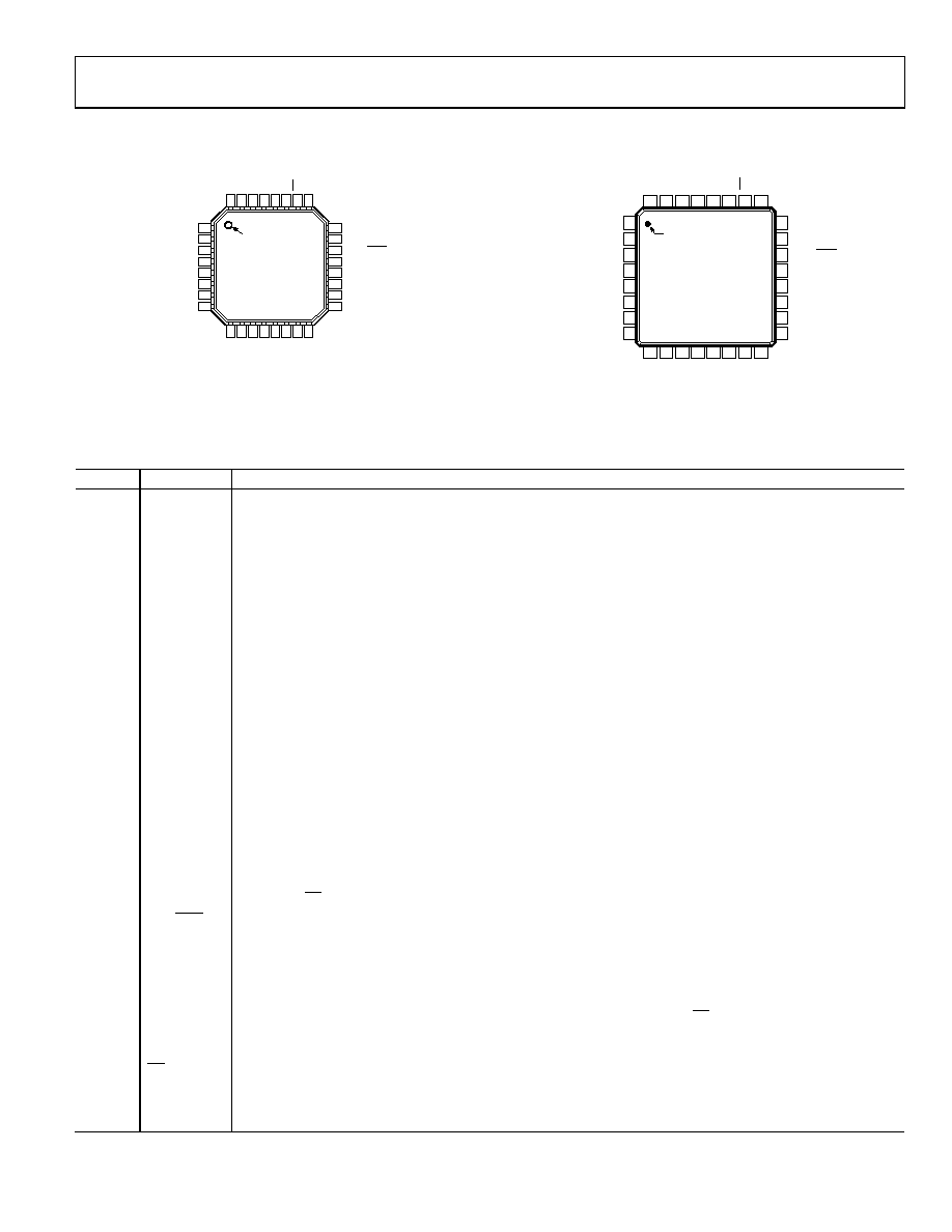
Figure 3. 32-Lead SU-32-2
Figure 2. 32-Lead CP-32-2
Table 4. Pin Function Descriptions
Pin No.
Mnemonic
Description
1, 29
DGND
Digital Ground. This is the ground reference point for all digital circuitry on the AD7265. Both DGND pins should
connect to the DGND plane of a system. The DGND and AGND voltages should ideally be at the same potential
and must not be more than 0.3 V apart, even on a transient basis.
2
REF SELECT
Internal/External Reference Selection. Logic input. If this pin is tied to DGND, the on-chip 2.5 V reference is used
as the reference source for both ADC A and ADC B. In addition, Pin D
A and Pin D
CAP
B must be tied to
decoupling capacitors. If the REF SELECT pin is tied to a logic high, an external reference can be supplied to the
AD7265 through the D
A pin and/or the D
B pin.
CAP
3
AVDD
Analog Supply Voltage, 2.7 V to 5.25 V. This is the only supply voltage for all analog circuitry on the AD7265. The
AV
and DV
DD
voltages should ideally be at the same potential and must not be more than 0.3 V apart, even on a
transient basis. This supply should be decoupled to AGND.
4, 20
D
A, D
B
CAP
Decoupling Capacitor Pins. Decoupling capacitors (470 nF recommended) are connected to these pins to
decouple the reference buffer for each respective ADC. Provided the output is buffered, the on-chip reference
can be taken from these pins and applied externally to the rest of a system. The range of the external reference is
dependent on the analog input range selected.
5, 6, 19
AGND
Analog Ground. Ground reference point for all analog circuitry on the AD7265. All analog input signals and any
external reference signal should be referred to this AGND voltage. All three of these AGND pins should connect
to the AGND plane of a system. The AGND and DGND voltages ideally should be at the same potential and must
not be more than 0.3 V apart, even on a transient basis.
7 to 12
V to V
A1
A6
Analog Inputs of ADC A. These may be programmed as six single-ended channels or three true differential
analog input channel pairs. See Table 6.
13 to 18
VB6 to VB1
Analog Inputs of ADC B. These may be programmed as six single-ended channels or three true differential
analog input channel pairs. See Table 6.
21
RANGE
Analog Input Range Selection. Logic input. The polarity on this pin determines the input range of the analog
input channels. If this pin is tied to a logic low, the analog input range is 0 V to VREF. If this pin is tied to a logic
high when CS goes low, the analog input range is 2 × V . See the Analog Input Selection section for details.
REF
22
SGL/DIFF
Logic Input. This pin selects whether the analog inputs are configured as differential pairs or single ended. A
logic low selects differential operation while a logic high selects single-ended operation. See the Analog Input
Selection section for details.
23 to 25
A2 to A0
Multiplexer Select. Logic inputs. These inputs are used to select the pair of channels to be simultaneously
converted, such as Channel 1 of both ADC A and ADC B, Channel 2 of both ADC A and ADC B, and so on. The pair
of channels selected may be two single-ended channels or two differential pairs. The logic states of these pins
need to be set up prior to the acquisition time and subsequent falling edge of CS to correctly set up the
multiplexer for that conversion. See the Analog Input Selection section for further details and Table 6 for
multiplexer address decoding.
26
CS
Chip Select. Active low logic input. This input provides the dual function of initiating conversions on the AD7265
and framing the serial data transfer.
27
SCLK
Serial Clock. Logic input. A serial clock input provides the SCLK for accessing the data from the AD7265. This
clock is also used as the clock source for the conversion process.
相关PDF资料 |
PDF描述 |
|---|---|
| VE-J11-MY-F1 | CONVERTER MOD DC/DC 12V 50W |
| MS3102E22-18S | CONN RCPT 8POS BOX MNT W/SCKT |
| VE-J42-MW-F2 | CONVERTER MOD DC/DC 15V 100W |
| VI-JVY-MY-F1 | CONVERTER MOD DC/DC 3.3V 33W |
| VE-J42-MW-F1 | CONVERTER MOD DC/DC 15V 100W |
相关代理商/技术参数 |
参数描述 |
|---|---|
| AD7265BCPZ-REEL | 功能描述:IC ADC 12BIT 3CHAN 1MSPS 32LFCSP RoHS:是 类别:集成电路 (IC) >> 数据采集 - 模数转换器 系列:- 标准包装:2,500 系列:- 位数:16 采样率(每秒):15 数据接口:MICROWIRE?,串行,SPI? 转换器数目:1 功率耗散(最大):480µW 电压电源:单电源 工作温度:-40°C ~ 85°C 安装类型:表面贴装 封装/外壳:38-WFQFN 裸露焊盘 供应商设备封装:38-QFN(5x7) 包装:带卷 (TR) 输入数目和类型:16 个单端,双极;8 个差分,双极 配用:DC1011A-C-ND - BOARD DELTA SIGMA ADC LTC2494 |
| AD7265BCPZ-REEL7 | 功能描述:IC ADC 12BIT 3CHAN 1MSPS 32LFCSP RoHS:是 类别:集成电路 (IC) >> 数据采集 - 模数转换器 系列:- 标准包装:2,500 系列:- 位数:16 采样率(每秒):15 数据接口:MICROWIRE?,串行,SPI? 转换器数目:1 功率耗散(最大):480µW 电压电源:单电源 工作温度:-40°C ~ 85°C 安装类型:表面贴装 封装/外壳:38-WFQFN 裸露焊盘 供应商设备封装:38-QFN(5x7) 包装:带卷 (TR) 输入数目和类型:16 个单端,双极;8 个差分,双极 配用:DC1011A-C-ND - BOARD DELTA SIGMA ADC LTC2494 |
| AD7265BSU | 制造商:AD 制造商全称:Analog Devices 功能描述:Differential Input, Dual 1 MSPS, 12-Bit, 3-Channel SAR ADC |
| AD7265BSUZ | 功能描述:IC ADC 12BIT 3CHAN 1MSPS 32TQFP RoHS:是 类别:集成电路 (IC) >> 数据采集 - 模数转换器 系列:- 其它有关文件:TSA1204 View All Specifications 标准包装:1 系列:- 位数:12 采样率(每秒):20M 数据接口:并联 转换器数目:2 功率耗散(最大):155mW 电压电源:模拟和数字 工作温度:-40°C ~ 85°C 安装类型:表面贴装 封装/外壳:48-TQFP 供应商设备封装:48-TQFP(7x7) 包装:Digi-Reel® 输入数目和类型:4 个单端,单极;2 个差分,单极 产品目录页面:1156 (CN2011-ZH PDF) 其它名称:497-5435-6 |
| AD7265BSUZ-REEL | 功能描述:IC ADC 12BIT 3CHAN 1MSPS 32TQFP RoHS:是 类别:集成电路 (IC) >> 数据采集 - 模数转换器 系列:- 标准包装:2,500 系列:- 位数:16 采样率(每秒):15 数据接口:MICROWIRE?,串行,SPI? 转换器数目:1 功率耗散(最大):480µW 电压电源:单电源 工作温度:-40°C ~ 85°C 安装类型:表面贴装 封装/外壳:38-WFQFN 裸露焊盘 供应商设备封装:38-QFN(5x7) 包装:带卷 (TR) 输入数目和类型:16 个单端,双极;8 个差分,双极 配用:DC1011A-C-ND - BOARD DELTA SIGMA ADC LTC2494 |
发布紧急采购,3分钟左右您将得到回复。