- 您现在的位置:买卖IC网 > PDF目录10681 > AD7274BUJZ-500RL7 (Analog Devices Inc)IC ADC 12BIT 3MSPS TSOT23-8 PDF资料下载
参数资料
| 型号: | AD7274BUJZ-500RL7 |
| 厂商: | Analog Devices Inc |
| 文件页数: | 3/29页 |
| 文件大小: | 0K |
| 描述: | IC ADC 12BIT 3MSPS TSOT23-8 |
| 标准包装: | 1 |
| 位数: | 12 |
| 采样率(每秒): | 3M |
| 数据接口: | DSP,MICROWIRE?,QSPI?,串行,SPI? |
| 转换器数目: | 1 |
| 功率耗散(最大): | 18mW |
| 电压电源: | 单电源 |
| 工作温度: | -40°C ~ 125°C |
| 安装类型: | 表面贴装 |
| 封装/外壳: | SOT-23-8 薄型,TSOT-23-8 |
| 供应商设备封装: | TSOT-23-8 |
| 包装: | 标准包装 |
| 输入数目和类型: | 1 个单端,单极 |
| 其它名称: | AD7274BUJZ-500RL7DKR |
第1页第2页当前第3页第4页第5页第6页第7页第8页第9页第10页第11页第12页第13页第14页第15页第16页第17页第18页第19页第20页第21页第22页第23页第24页第25页第26页第27页第28页第29页
AD7273/AD7274
Rev. 0 | Page 10 of 28
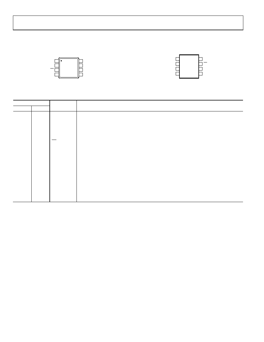
PIN CONFIGURATIONS AND FUNCTION DESCRIPTIONS
VDD 1
SDATA
2
CS
3
AGND
4
VIN
8
DGND
7
SCLK
6
VREF
5
AD7273/
AD7274
TOP VIEW
(Not to Scale)
04973-008
Figure 8. 8-Lead MSOP Pin Configuration
VDD
VIN
1
SDATA
2
3
4
8
7
6
5
DGND
AGND
CS
SCLK
VREF
AD7273/
AD7274
TOP VIEW
(Not to Scale)
04973-009
Figure 9. 8-Lead TSOT Pin Configuration
Table 6. Pin Function Descriptions
Pin No.
MSOP
TSOT
Mnemonic
Description
1
VDD
Power Supply Input. The VDD range for the AD7273/AD7274 is from 2.35 V to 3.6 V.
2
SDATA
Data Out. Logic output. The conversion result from the AD7273/AD7274 is provided on this output as a
serial data stream. The bits are clocked out on the falling edge of the SCLK input. The data stream from
the AD7274 consists of two leading zeros followed by the 12 bits of conversion data and two trailing
zeros, provided MSB first. The data stream from the AD7273 consists of two leading zeros followed
by the 10 bits of conversion data and four trailing zeros, provided MSB first.
3
7
CS
Chip Select. Active low logic input. This input provides the dual function of initiating conversion on
the AD7273/AD7274 and framing the serial data transfer.
4
8
AGND
Analog Ground. Ground reference point for all circuitry on the AD7273/AD7274. All analog signals
and any external reference signal should be referred to this AGND voltage.
5
VREF
Voltage Reference Input. This pin becomes the reference voltage input. An external reference should
be applied at this pin. The external reference input range is 1.4 V to VDD. A 10 μF capacitor should be
tied between this pin and AGND.
6
SCLK
Serial Clock. Logic input. SCLK provides the serial clock for accessing data from the part. This clock
input is also used as the clock source for the conversion process of AD7273/AD7274.
7
3
DGND
Digital Ground. Ground reference point for all digital circuitry on the AD7273/AD7274. The DGND and
AGND voltages ideally should be at the same potential and must not be more than 0.3 V apart, even
on a transient basis.
8
4
VIN
Analog Input. Single-ended analog input channel. The input range is 0 to VREF.
相关PDF资料 |
PDF描述 |
|---|---|
| VI-22Y-IV-B1 | CONVERTER MOD DC/DC 3.3V 99W |
| VI-201-IX-B1 | CONVERTER MOD DC/DC 12V 75W |
| LT1116CS8#TR | IC COMPARATOR 12NS SINGLE 8SOIC |
| AD8564ARZ-REEL | IC COMPARATOR QUAD 7NS 16SOIC TR |
| AD96685BR-REEL | IC COMP SNGL ULTRA-FAST 16-SOIC |
相关代理商/技术参数 |
参数描述 |
|---|---|
| AD7274BUJZ-500RL72 | 制造商:AD 制造商全称:Analog Devices 功能描述:3 MSPS,10-/12-Bit ADCs in 8-Lead TSOT |
| AD7274BUJZ-REEL7 | 功能描述:IC ADC 12BIT 3MSPS TSOT23-8 RoHS:是 类别:集成电路 (IC) >> 数据采集 - 模数转换器 系列:- 标准包装:1,000 系列:- 位数:16 采样率(每秒):45k 数据接口:串行 转换器数目:2 功率耗散(最大):315mW 电压电源:模拟和数字 工作温度:0°C ~ 70°C 安装类型:表面贴装 封装/外壳:28-SOIC(0.295",7.50mm 宽) 供应商设备封装:28-SOIC W 包装:带卷 (TR) 输入数目和类型:2 个单端,单极 |
| AD7274BUJZ-REEL72 | 制造商:AD 制造商全称:Analog Devices 功能描述:3 MSPS,10-/12-Bit ADCs in 8-Lead TSOT |
| AD7276 | 制造商:AD 制造商全称:Analog Devices 功能描述:3MSPS,12-/10-/8-Bit ADCs in 6-Lead TSOT |
| AD7276ARMZ | 功能描述:IC ADC 12BIT 3MSPS 8MSOP RoHS:是 类别:集成电路 (IC) >> 数据采集 - 模数转换器 系列:- 标准包装:1 系列:microPOWER™ 位数:8 采样率(每秒):1M 数据接口:串行,SPI? 转换器数目:1 功率耗散(最大):- 电压电源:模拟和数字 工作温度:-40°C ~ 125°C 安装类型:表面贴装 封装/外壳:24-VFQFN 裸露焊盘 供应商设备封装:24-VQFN 裸露焊盘(4x4) 包装:Digi-Reel® 输入数目和类型:8 个单端,单极 产品目录页面:892 (CN2011-ZH PDF) 其它名称:296-25851-6 |
发布紧急采购,3分钟左右您将得到回复。