参数资料
| 型号: | AD7276BRM |
| 厂商: | Analog Devices Inc |
| 文件页数: | 16/29页 |
| 文件大小: | 0K |
| 描述: | IC ADC 12BIT 3MSPS HS LP 8MSOP |
| 标准包装: | 50 |
| 位数: | 12 |
| 采样率(每秒): | 3M |
| 数据接口: | DSP,MICROWIRE?,QSPI?,串行,SPI? |
| 转换器数目: | 1 |
| 功率耗散(最大): | 19.8mW |
| 电压电源: | 单电源 |
| 工作温度: | -40°C ~ 125°C |
| 安装类型: | 表面贴装 |
| 封装/外壳: | 8-TSSOP,8-MSOP(0.118",3.00mm 宽) |
| 供应商设备封装: | 8-MSOP |
| 包装: | 管件 |
| 输入数目和类型: | 1 个单端,单极 |
| 配用: | EVAL-AD7276CBZ-ND - BOARD EVALUATION FOR AD7276 |
第1页第2页第3页第4页第5页第6页第7页第8页第9页第10页第11页第12页第13页第14页第15页当前第16页第17页第18页第19页第20页第21页第22页第23页第24页第25页第26页第27页第28页第29页
AD7276/AD7277/AD7278
Rev. C | Page 22 of 28
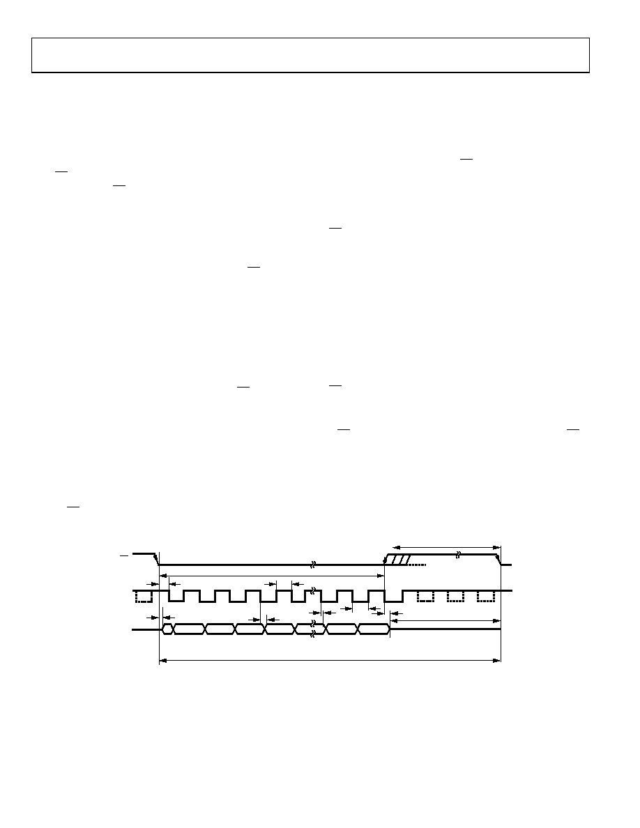
SERIAL INTERFACE
for serial interfacing to the AD7276, AD7277, and AD7278. The
serial clock provides the conversion clock and controls the transfer
of information from the AD7276/AD7277/AD7278 during
conversion.
The CS signal initiates the data transfer and conversion process.
The falling edge of CS puts the track-and-hold into hold mode
and takes the bus out of three-state. The analog input is sampled
and the conversion is initiated at this point.
For the AD7276, the conversion requires completing 14 SCLK
cycles. Once 13 SCLK falling edges have elapsed, the track-and-
hold goes back into track mode on the next SCLK rising edge,
as shown in Figure 31 at Point B. If the rising edge of CS occurs
before 14 SCLKs have elapsed, the conversion is terminated and
the SDATA line goes back into three-state. If 16 SCLKs are
considered in the cycle, the last two bits are zeros and SDATA
returns to three-state on the 16th SCLK falling edge, as shown in
.
For the AD7277, the conversion requires completing 12 SCLK
cycles. Once 11 SCLK falling edges elapse, the track-and-hold
goes back into track mode on the next SCLK rising edge, as
shown in Figure 33 at Point B. If the rising edge of CS occurs
before 12 SCLKs elapse, the conversion is terminated and the
SDATA line goes back into three-state. If 16 SCLKs are considered
in the cycle, the AD7277 clocks out four trailing zeros for the
last four bits and SDATA returns to three-state on the 16th SCLK
falling edge, as shown in
.
For the AD7278, the conversion requires completing 10 SCLK
cycles. Once 9 SCLK falling edges elapse, the track-and-hold
goes back into track mode on the next rising edge. If the rising
edge of CS occurs before 10 SCLKs elapse, the part enters power-
down mode.
If 16 SCLKs are considered in the cycle, then the AD7278 clocks
out six trailing zeros for the last six bits and SDATA returns to
If the user considers a 14 SCLK cycle serial interface for the
AD7276/AD7277/AD7278, then CS must be brought high after
the 14th SCLK falling edge. Then the last two trailing zeros are
ignored, and SDATA goes back into three-state. In this case, the
3 MSPS throughput can be achieved by using a 48 MHz clock
frequency.
CS going low clocks out the first leading zero to be read by the
microcontroller or DSP. The remaining data is then clocked out
by subsequent SCLK falling edges, beginning with the second
leading zero. Therefore, the first falling clock edge on the serial
clock provides the first leading zero and clocks out the second
leading zero. The final bit in the data transfer is valid on the 16th
falling edge, because it is clocked out on the previous (15th)
falling edge.
In applications with a slower SCLK, it is possible to read data on
each SCLK rising edge. In such cases, the first falling edge of SCLK
clocks out the second leading zero and can be read on the first
rising edge. However, the first leading zero clocked out when
CS goes low is missed if read within the first falling edge. The
15th falling edge of SCLK clocks out the last bit and can be read
on the 15th rising SCLK edge.
If CS goes low just after one SCLK falling edge elapses, then CS
clocks out the first leading zero and can be read on the SCLK
rising edge. The next SCLK falling edge clocks out the second
leading zero and can be read on the following rising edge.
04
90
3-
0
99
tQUIET
tCONVERT
1/THROUGHPUT
CS
15
13
t4
23
4
t5
t3
t2
t6
t7
t9
14
B
t1
SCLK
SDATA
THREE-STATE
THREE-
STATE
2 LEADING
ZEROS
ZZERO
DB11
DB10
DB9
DB1
DB0
Figure 31. AD7276 Serial Interface Timing Diagram 14 SCLK Cycle
相关PDF资料 |
PDF描述 |
|---|---|
| AD7291BCPZ-RL7 | IC ADC I2C/SRL 22.22K 20LFCSP |
| AD7298-1BCPZ-RL | IC ADC 10BIT SPI/SRL 8CH 20LFCSP |
| AD7298BCPZ-RL7 | IC ADC 10BIT SPI/SRL 8CH 20LFCSP |
| AD7302BRUZ-REEL7 | IC DAC 8BIT DUAL R-R 20-TSSOP |
| AD7303BRM | IC DAC 8BIT DUAL R-R 8-MSOP |
相关代理商/技术参数 |
参数描述 |
|---|---|
| AD7276BRM-U2 | 制造商:Analog Devices 功能描述:ADC SGL SAR 3MSPS 12-BIT SERL 8MSOP - Bulk |
| AD7276BRMZ | 功能描述:IC ADC 12BIT SRL 3MSPS 8MSOP RoHS:是 类别:集成电路 (IC) >> 数据采集 - 模数转换器 系列:- 其它有关文件:TSA1204 View All Specifications 标准包装:1 系列:- 位数:12 采样率(每秒):20M 数据接口:并联 转换器数目:2 功率耗散(最大):155mW 电压电源:模拟和数字 工作温度:-40°C ~ 85°C 安装类型:表面贴装 封装/外壳:48-TQFP 供应商设备封装:48-TQFP(7x7) 包装:Digi-Reel® 输入数目和类型:4 个单端,单极;2 个差分,单极 产品目录页面:1156 (CN2011-ZH PDF) 其它名称:497-5435-6 |
| AD7276BRMZ-REEL | 功能描述:IC ADC 12BIT 3MSPS HS LP 8MSOP RoHS:是 类别:集成电路 (IC) >> 数据采集 - 模数转换器 系列:- 标准包装:1,000 系列:- 位数:16 采样率(每秒):45k 数据接口:串行 转换器数目:2 功率耗散(最大):315mW 电压电源:模拟和数字 工作温度:0°C ~ 70°C 安装类型:表面贴装 封装/外壳:28-SOIC(0.295",7.50mm 宽) 供应商设备封装:28-SOIC W 包装:带卷 (TR) 输入数目和类型:2 个单端,单极 |
| AD7276BUJ-REEL | 制造商:AD 制造商全称:Analog Devices 功能描述:3MSPS,12-/10-/8-Bit ADCs in 6-Lead TSOT |
| AD7276BUJZ | 制造商:Analog Devices 功能描述:IC,12-bit ADC,AD7276BUJZ |
发布紧急采购,3分钟左右您将得到回复。