参数资料
| 型号: | AD7305BR |
| 厂商: | Analog Devices Inc |
| 文件页数: | 7/20页 |
| 文件大小: | 0K |
| 描述: | IC DAC 8BIT QUAD 5V R-R 20-SOIC |
| 产品培训模块: | Data Converter Fundamentals DAC Architectures |
| 标准包装: | 37 |
| 设置时间: | 1µs |
| 位数: | 8 |
| 数据接口: | 并联 |
| 转换器数目: | 4 |
| 电压电源: | 双 ± |
| 功率耗散(最大): | 60mW |
| 工作温度: | -40°C ~ 85°C |
| 安装类型: | 表面贴装 |
| 封装/外壳: | 20-SOIC(0.295",7.50mm 宽) |
| 供应商设备封装: | 20-SOIC W |
| 包装: | 管件 |
| 输出数目和类型: | 4 电压,单极;4 电压,双极 |
| 采样率(每秒): | 1M |
AD7304/AD7305
Rev. C | Page 15 of 20
AD7304 SERIAL DATA INTERFACE
The AD7304 uses a 3-wire (CS, SDI, CLK) SPI-compatible
serial data interface. New serial data is clocked into the serial
input register in a 12-bit data-word format. MSB bits are loaded
first.
Table 5 defines the 12 data-word bits. Data is placed on the
SDI/SHDN pin and clocked into the register on the positive
clock edge of CLK subject to the data setup and data hold time
requirements specified in the Timing Specifications section.
Data can only be clocked in while the CS chip select pin is
active low. Only the last 12-bits clocked into the serial register
are interrogated when the CS pin returns to the logic high state,
extra data bits are ignored. Since most microcontrollers output
serial data in 8-bit bytes, two right-justified data bytes can be
written to the AD7304. Keeping the CS line low between the
first and second byte transfer results in a successful serial
register update.
Once the data is properly aligned in the shift register, the
positive edge of the CS initiates either the transfer of new data
to the target DAC register, determined by the decoding of
Address Bits A1 and A0, or the shutdown features is activated
based on the SAC or SDC bits. When either SAC or SDC pins
are set (Logic 0), the loading of new data determined by Bits B9
to B0 are still loaded, but the results do not appear on the buffer
outputs until the device is brought out of the shutdown state.
The selected DAC output voltages become high impedance with
a nominal resistance of 120 k to ground, see Figure 34. If
both the SAC and SDC pins are set, all channels are still placed
in shutdown mode. When the AD7304 has been programmed
into the power shutdown state, the present DAC register data is
maintained as long as VDD remains greater than 2.7 V. The
remaining characteristics of the software serial interface are
defined by Table 4, Table 5, and Figure 5.
Two additional pins, CLR and LDAC, on the AD7304 provide
hardware control over the clear function and the DAC register
loading. If these functions are not needed, the CLR pin can be
tied to logic high, and the LDAC pin can be tied to logic low.
The asynchronous input CLR pin forces all input and DAC
registers to the zero-code state. The asynchronous LDAC pin
can be strobed to active low when all DAC registers need to be
updated simultaneously from their respective input registers.
The LDAC pin places the DAC register in a transparent mode
while in the logic low state.
AD7304
DAC A
B
C
D
2:4
DECODE
A0
A1
SDC
SAC
D0
D1
D2
D3
D4
D5
D6
D7
8
EN
320k
280k
80k
640k
680k
VDD
LDAC
VSS
VOUTC
CS
SDI
VOUTB
VOUTA
VDD
DQ
INPUT
REGISTER R
POWER-
ON
RESET
VREFA
VREFB
VREFC
VREFD
VOUTD
CLR
GND
CLK
INPUT
REGISTER R
R
DQ
OE
DAC A
REGISTER
DAC B
OE
DAC B
REGISTER
DAC C
OE
DAC C
REGISTER
DAC D
OE
DAC D
REGISTER
01114-035
INPUT
REGISTER
INPUT
REGISTER
R
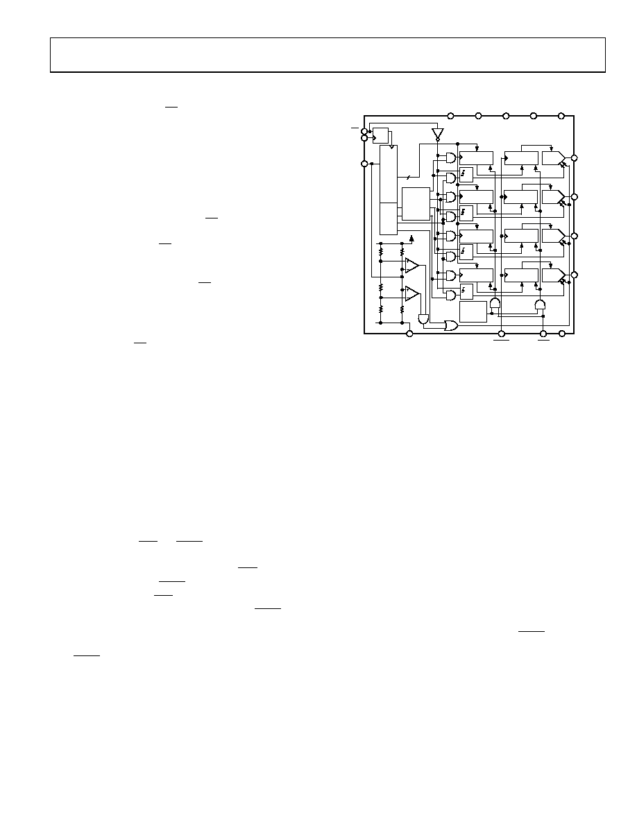
Figure 35. AD7304 Equivalent Logic Interface
AD7304 HARDWARE SHUTDOWN SHDN
If a three-state driver is used on the SDI/SHDN pin, the
AD7304 can be placed into a power shutdown mode when the
SDI/ SHDN pin is placed in a high impedance state. For proper
operation, no other termination voltages should be present on
this pin. An internal window comparator detects when the logic
voltage on the SHDN pin is between 28% and 36% of VDD. A
high impedance internal bias generator provides this voltage on
the SHDN pin. The four DAC output voltages become high
impedance with a nominal resistance of 120 k to ground (see
Figure 34 for an equivalent circuit).
AD7304/AD7305 POWER-ON RESET
When the VDD power supply is turned on, an internal reset
strobe forces all the input and DAC registers to the zero-code
state. The VDD power supply should have a monotonically
increasing ramp in order to have consistent results, especially in
the region of VDD = 1.5 V to 2.3 V. The VSS supply has no effect
on the power-on reset performance. The DAC register data
stays at zero until a valid serial register software load takes
place. In the case of the double-buffered AD7305, the output
DAC register can only be changed once the LDAC strobe is
initiated.
POWER-UP SEQUENCE
It is recommended to power VDD/VSS first before applying any
voltage to the reference terminals to avoid potential latch up.
The ideal power-up sequence is in the following order: GND,
VDD, VSS, Digital Inputs, and VREFx. The order of powering
digital inputs and reference inputs is not important as long as
they are powered after VDD/VSS.
相关PDF资料 |
PDF描述 |
|---|---|
| AD7533KR | IC DAC 10BIT MULTIPLYING 16-SOIC |
| AD7945BN | IC DAC 12BIT MULT PARALL 20-DIP |
| AD7943BN | IC DAC 12BIT MULT SRL 16-DIP |
| AD7804BRZ-REEL | IC DAC 10BIT QUAD SRL 16-SOIC |
| AD5328ARUZ-REEL7 | IC DAC 12BIT OCTAL W/BUF 16TSSOP |
相关代理商/技术参数 |
参数描述 |
|---|---|
| AD7305BR-REEL | 功能描述:IC DAC 8BIT QUAD R-R 20-SOIC RoHS:否 类别:集成电路 (IC) >> 数据采集 - 数模转换器 系列:- 产品培训模块:LTC263x 12-, 10-, and 8-Bit VOUT DAC Family 特色产品:LTC2636 - Octal 12-/10-/8-Bit SPI VOUT DACs with 10ppm/°C Reference 标准包装:91 系列:- 设置时间:4µs 位数:10 数据接口:MICROWIRE?,串行,SPI? 转换器数目:8 电压电源:单电源 功率耗散(最大):2.7mW 工作温度:-40°C ~ 85°C 安装类型:表面贴装 封装/外壳:14-WFDFN 裸露焊盘 供应商设备封装:14-DFN-EP(4x3) 包装:管件 输出数目和类型:8 电压,单极 采样率(每秒):* |
| AD7305BR-REEL7 | 功能描述:INTEGRATED CIRCUIT 制造商:analog devices inc. 系列:* 包装:带卷(TR) 零件状态:最後搶購 封装/外壳:20-SOIC(0.295",7.50mm 宽) 供应商器件封装:20-SOIC 标准包装:1 |
| AD7305BRU | 功能描述:IC DAC 8BIT QUAD R-R 20-TSSOP RoHS:否 类别:集成电路 (IC) >> 数据采集 - 数模转换器 系列:- 标准包装:47 系列:- 设置时间:2µs 位数:14 数据接口:并联 转换器数目:1 电压电源:单电源 功率耗散(最大):55µW 工作温度:-40°C ~ 85°C 安装类型:表面贴装 封装/外壳:28-SSOP(0.209",5.30mm 宽) 供应商设备封装:28-SSOP 包装:管件 输出数目和类型:1 电流,单极;1 电流,双极 采样率(每秒):* |
| AD7305BRU-REEL7 | 功能描述:IC DAC 8BIT QUAD R-R 20-TSSOP RoHS:否 类别:集成电路 (IC) >> 数据采集 - 数模转换器 系列:- 产品培训模块:LTC263x 12-, 10-, and 8-Bit VOUT DAC Family 特色产品:LTC2636 - Octal 12-/10-/8-Bit SPI VOUT DACs with 10ppm/°C Reference 标准包装:91 系列:- 设置时间:4µs 位数:10 数据接口:MICROWIRE?,串行,SPI? 转换器数目:8 电压电源:单电源 功率耗散(最大):2.7mW 工作温度:-40°C ~ 85°C 安装类型:表面贴装 封装/外壳:14-WFDFN 裸露焊盘 供应商设备封装:14-DFN-EP(4x3) 包装:管件 输出数目和类型:8 电压,单极 采样率(每秒):* |
| AD7305BRUZ | 功能描述:IC DAC 8BIT QUAD R-R 20-TSSOP RoHS:是 类别:集成电路 (IC) >> 数据采集 - 数模转换器 系列:- 产品培训模块:Lead (SnPb) Finish for COTS Obsolescence Mitigation Program 标准包装:50 系列:- 设置时间:4µs 位数:12 数据接口:串行 转换器数目:2 电压电源:单电源 功率耗散(最大):- 工作温度:-40°C ~ 85°C 安装类型:表面贴装 封装/外壳:8-TSSOP,8-MSOP(0.118",3.00mm 宽) 供应商设备封装:8-uMAX 包装:管件 输出数目和类型:2 电压,单极 采样率(每秒):* 产品目录页面:1398 (CN2011-ZH PDF) |
发布紧急采购,3分钟左右您将得到回复。