参数资料
| 型号: | AD7305BRU |
| 厂商: | Analog Devices Inc |
| 文件页数: | 1/20页 |
| 文件大小: | 0K |
| 描述: | IC DAC 8BIT QUAD R-R 20-TSSOP |
| 产品培训模块: | Data Converter Fundamentals DAC Architectures |
| 标准包装: | 75 |
| 设置时间: | 1µs |
| 位数: | 8 |
| 数据接口: | 并联 |
| 转换器数目: | 4 |
| 电压电源: | 双 ± |
| 功率耗散(最大): | 60mW |
| 工作温度: | -40°C ~ 85°C |
| 安装类型: | 表面贴装 |
| 封装/外壳: | 20-TSSOP(0.173",4.40mm 宽) |
| 供应商设备封装: | 20-TSSOP |
| 包装: | 管件 |
| 输出数目和类型: | 4 电压,单极;4 电压,双极 |
| 采样率(每秒): | 1M |
3 V/5 V, Rail-to-Rail
Quad, 8-Bit DAC
AD7304/AD7305
Rev. C
Information furnished by Analog Devices is believed to be accurate and reliable.
However, no responsibility is assumed by Analog Devices for its use, nor for any
infringements of patents or other rights of third parties that may result from its use.
Specifications subject to change without notice. No license is granted by implication
or otherwise under any patent or patent rights of Analog Devices. Trademarks and
registered trademarks are the property of their respective owners.
One Technology Way, P.O. Box 9106, Norwood, MA 02062-9106, U.S.A.
Tel: 781.329.4700
Fax: 781.326.8703
2004 Analog Devices, Inc. All rights reserved.
FEATURES
Four 8-bit DACs in one package
+3 V, +5 V, and ±5 V operation
Rail-to-rail REF input to voltage output swing
2.6 MHz reference multiplying bandwidth
Internal power-on reset
SPI serial interface-compatible—AD7304
Fast parallel interface—AD7305
40 A power shutdown
APPLICATIONS
Automotive output span voltage
Instrumentation, digitally controlled calibration
Pin-compatible AD7226 replacement when VDD < 5.5 V
GENERAL DESCRIPTION
The AD7304/AD73051 are quad, 8-bit DACs that operate from
a single +3 V to +5 V supply, or ±5 V supplies. The AD7304 has
a serial interface, while the AD7305 has a parallel interface.
Internal precision buffers swing rail-to-rail. The reference input
range includes both supply rails, allowing for positive or negative
full-scale output voltages. Operation is guaranteed over the
supply voltage range of 2.7 V to 5.5 V, consuming less than
9 mW from a 3 V supply.
The full-scale voltage output is determined by the external
reference input voltage applied. The rail-to-rail VREF input to
DAC VOUT allows for a full-scale voltage set equal to the positive
supply, VDD, the negative supply, VSS, or any value in between.
The AD7304’s doubled-buffered serial data interface offers high
speed, 3-wire, SPI-, and microcontroller-compatible inputs
using data in (SDI), clock (CLK), and chip select (CS) pins.
Additionally, an internal power-on reset sets the output to zero
scale.
The parallel input AD7305 uses a standard address decode
along with the WR control line to load data into the input
registers.
The double-buffered architecture allows all four input registers
to be preloaded with new values, followed by an LDAC control
strobe that copies all the new data into the DAC registers,
thereby updating the analog output values.
_____________________________________________________
1 Protected under Patent No. 5684481.
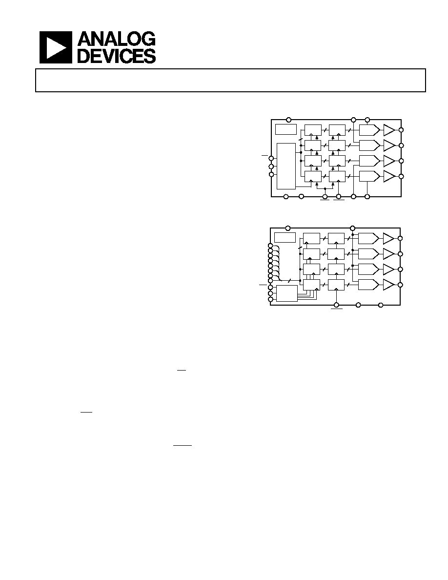
FUNCTIONAL BLOCK DIAGRAMS
CS
PWR-ON
RESET
VSS
AD7304
VOUTA
INPUT
REG A
DAC A
LDAC
SDI/SHDN
GND
CLK
8
DAC A
REG
DAC B
8
DAC D
DAC C
SERIAL
REG
VREFB VREFA
CLR
VREFCVREFD
VDD
VOUTB
VOUTC
VOUTD
INPUT
REG B
DAC B
REG
INPUT
REG C
DAC C
REG
INPUT
REG D
DAC D
REG
01114-001
Figure 1.
PWR-ON
RESET
AD7305
VOUTA
INPUT
REG A
DAC A
LDAC
8
DAC A
REG
DAC B
8
DAC D
DAC C
DECODE
VREF
VSS
GND
VDD
VOUTB
VOUTC
VOUTD
INPUT
REG B
DAC B
REG
INPUT
REG C
DAC C
REG
INPUT
REG D
DAC D
REG
01114-002
DB0
DB1
DB2
DB3
DB4
DB5
DB6
8
WR
A0/SHDN
A1
Figure 2.
When operating from less than 5.5 V, the AD7305 is
pin-compatible with the popular industry-standard AD7226.
An internal power-on reset places both parts in the zero-scale
state at turn-on. A 40 A power shutdown (SHDN) feature is
activated on both parts by three-stating the SDI/SHDN pin on
the AD7304 and three-stating the A0/SHDN address pin on the
AD7305.
The AD7304/AD7305 are specified over the extended industrial
40°C to +85°C and the automotive 40°C to +125°C
temperature ranges. AD7304s are available in a wide-body
16-lead SOIC (R-16) package. The parallel input AD7305 is
available in the wide-body 20-lead SOIC (R-20) surface-mount
package. For ultracompact applications, the thin 1.1 mm,
16-lead TSSOP (RU-16) package is available for the AD7304,
while the 20-lead TSSOP (RU-20) houses the AD7305.
相关PDF资料 |
PDF描述 |
|---|---|
| AD7321BRUZ-REEL7 | IC ADC 12BIT+ SAR 2CHAN 14TSSOP |
| AD7322BRUZ-REEL7 | IC ADC 12BIT+ SAR 2CHAN 14TSSOP |
| AD7323BRUZ-REEL7 | IC ADC 12BIT+ SAR 4CHAN 16TSSOP |
| AD7324BRUZ-REEL | IC ADC 12BIT+SAR 4CHAN 16-TSSOP |
| AD7327BRUZ-REEL7 | IC ADC 12BIT+ SAR 8CHAN 20TSSOP |
相关代理商/技术参数 |
参数描述 |
|---|---|
| AD7305BRU-REEL7 | 功能描述:IC DAC 8BIT QUAD R-R 20-TSSOP RoHS:否 类别:集成电路 (IC) >> 数据采集 - 数模转换器 系列:- 产品培训模块:LTC263x 12-, 10-, and 8-Bit VOUT DAC Family 特色产品:LTC2636 - Octal 12-/10-/8-Bit SPI VOUT DACs with 10ppm/°C Reference 标准包装:91 系列:- 设置时间:4µs 位数:10 数据接口:MICROWIRE?,串行,SPI? 转换器数目:8 电压电源:单电源 功率耗散(最大):2.7mW 工作温度:-40°C ~ 85°C 安装类型:表面贴装 封装/外壳:14-WFDFN 裸露焊盘 供应商设备封装:14-DFN-EP(4x3) 包装:管件 输出数目和类型:8 电压,单极 采样率(每秒):* |
| AD7305BRUZ | 功能描述:IC DAC 8BIT QUAD R-R 20-TSSOP RoHS:是 类别:集成电路 (IC) >> 数据采集 - 数模转换器 系列:- 产品培训模块:Lead (SnPb) Finish for COTS Obsolescence Mitigation Program 标准包装:50 系列:- 设置时间:4µs 位数:12 数据接口:串行 转换器数目:2 电压电源:单电源 功率耗散(最大):- 工作温度:-40°C ~ 85°C 安装类型:表面贴装 封装/外壳:8-TSSOP,8-MSOP(0.118",3.00mm 宽) 供应商设备封装:8-uMAX 包装:管件 输出数目和类型:2 电压,单极 采样率(每秒):* 产品目录页面:1398 (CN2011-ZH PDF) |
| AD7305BRUZ1 | 制造商:AD 制造商全称:Analog Devices 功能描述:3 V/5 V, Rail-to-Rail Quad, 8-Bit DAC |
| AD7305BRUZ-REEL7 | 功能描述:IC DAC 8BIT QUAD R-R 20-TSSOP RoHS:是 类别:集成电路 (IC) >> 数据采集 - 数模转换器 系列:- 产品培训模块:LTC263x 12-, 10-, and 8-Bit VOUT DAC Family 特色产品:LTC2636 - Octal 12-/10-/8-Bit SPI VOUT DACs with 10ppm/°C Reference 标准包装:91 系列:- 设置时间:4µs 位数:10 数据接口:MICROWIRE?,串行,SPI? 转换器数目:8 电压电源:单电源 功率耗散(最大):2.7mW 工作温度:-40°C ~ 85°C 安装类型:表面贴装 封装/外壳:14-WFDFN 裸露焊盘 供应商设备封装:14-DFN-EP(4x3) 包装:管件 输出数目和类型:8 电压,单极 采样率(每秒):* |
| AD7305BRUZ-REEL71 | 制造商:AD 制造商全称:Analog Devices 功能描述:3 V/5 V, Rail-to-Rail Quad, 8-Bit DAC |
发布紧急采购,3分钟左右您将得到回复。