- 您现在的位置:买卖IC网 > PDF目录10799 > AD7305YR (Analog Devices Inc)IC DAC 8BIT QUAD R-R 20-SOIC PDF资料下载
参数资料
| 型号: | AD7305YR |
| 厂商: | Analog Devices Inc |
| 文件页数: | 8/20页 |
| 文件大小: | 0K |
| 描述: | IC DAC 8BIT QUAD R-R 20-SOIC |
| 产品培训模块: | Data Converter Fundamentals DAC Architectures |
| 产品变化通告: | Product Discontinuance 27/Oct/2011 |
| 标准包装: | 37 |
| 设置时间: | 1µs |
| 位数: | 8 |
| 数据接口: | 并联 |
| 转换器数目: | 4 |
| 电压电源: | 双 ± |
| 功率耗散(最大): | 60mW |
| 工作温度: | -40°C ~ 85°C |
| 安装类型: | 表面贴装 |
| 封装/外壳: | 20-SOIC(0.295",7.50mm 宽) |
| 供应商设备封装: | 20-SOIC W |
| 包装: | 管件 |
| 输出数目和类型: | 4 电压,单极;4 电压,双极 |
| 采样率(每秒): | 1M |
AD7304/AD7305
Rev. C | Page 16 of 20
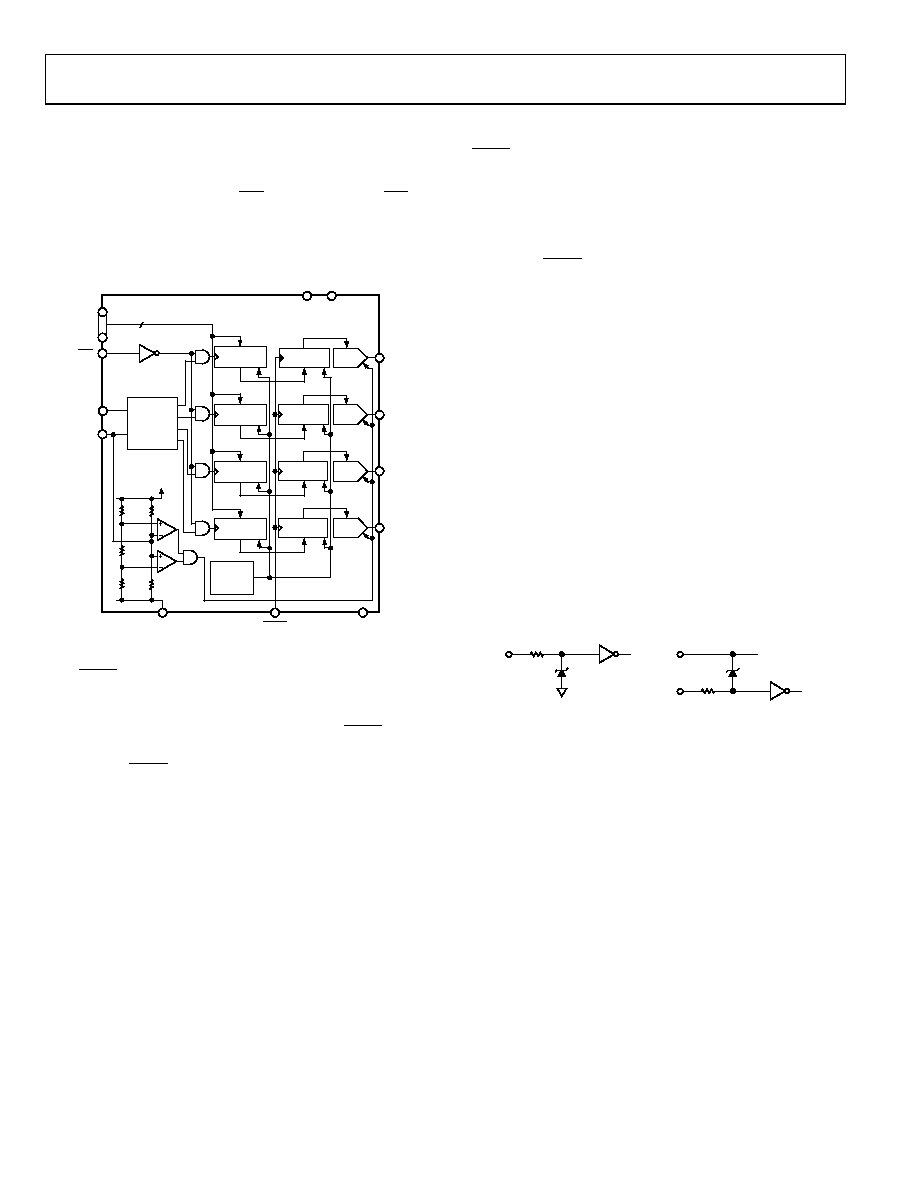
AD7305 PARALLEL DATA INTERFACE
The AD7305 has an 8-bit parallel interface DB7 = MSB, DB0 =
LSB. Two address bits, A1 and A0, are decoded when an active
low write strobe is placed on the WR pin, see Table 6. The WR
is a level-sensitive input pin, therefore, the data setup and data
hold times defined in the Timing Specifications section need to
be adhered to.
AD7305
8
320k
280k
80k
640k
680k
VDD
LDAC
VSS
WR
VDD
VREF
GND
DATA
DB0–DB7
A1
A0/SHDN
R
POWER-
ON
RESET
DAC A
OE
DAC A
REGISTER
DAC B
OE
DAC B
REGISTER
DAC C
OE
DAC C
REGISTER
DAC D
OE
DAC D
REGISTER
DAC A
B
C
D
2:4
DECODE
VOUTC
VOUTB
VOUTA
VOUTD
01114-036
INPUT
REGISTER
INPUT
REGISTER
INPUT
REGISTER
INPUT
REGISTER
R
Figure 36. AD7305 Equivalent Logic Interface
The LDAC pin provides the capability of simultaneously
updating all DAC registers with new data from the input
registers at the same time. This results in the analog outputs all
changing to their new values at the same time. The LDAC pin is
a level-sensitive input. If the simultaneous update feature is not
required, the LDAC pin can be tied to logic low. When the
LDAC is tied to Logic Low, the DAC registers become
transparent and the input register data determines the DAC
output voltage (see Figure 36 for an equivalent interface logic
diagram).
AD7226 PIN COMPATIBILITY
By tying the LDAC pin to ground, the AD7305 has the same pin
configuration and functionality as the AD7226, with the
exception of a lower power supply operating voltage.
AD7305 HARDWARE SHUTDOWN SHDN
If a three-state driver is used on the A0/SHDN pin, the AD7305
can be placed into a power shutdown mode when the A0/SHDN
pin is placed in a high impedance state. For proper operation,
no other termination voltages should be present on this pin. An
internal window comparator detects when the logic voltage on
the SHDN pin is between 28% and 36% of VDD. A high imped-
ance, internal-bias generator provides this voltage on the SHDN
pin. The four DAC output voltages become high impedance
with a nominal resistance of 120 k to ground.
ESD PROTECTION CIRCUITS
All logic input pins contain back-biased ESD protection Zeners
connected to ground (GND). The VREF pins also contain a back-
GND
DIGITAL
INPUTS
VDD
VREFX
01114-037
Figure 37. Equivalent ESD Protection Circuits
相关PDF资料 |
PDF描述 |
|---|---|
| LT1719CS6#TRMPBF | IC COMP R-RINOUT SINGLE SOT23-6 |
| AD7304BR-REEL | IC DAC 8BIT QUAD R-R 16-SOIC |
| LT1716HS5#TRMPBF | IC COMP OTT R-R 44V TSOT-23-5 |
| AD7304BR | IC DAC 8BIT QUAD R-R 16-SOIC |
| VE-J7L-MY-S | CONVERTER MOD DC/DC 28V 50W |
相关代理商/技术参数 |
参数描述 |
|---|---|
| AD7305YR-REEL | 制造商:Analog Devices 功能描述:DAC 4-CH R-2R 8-bit 20-Pin SOIC W T/R 制造商:Analog Devices 功能描述:DAC 4-CH R-2R 8BIT 20SOIC W - Tape and Reel |
| AD7305YRZ | 功能描述:IC DAC 8BIT QUAD R-R 20SOIC RoHS:是 类别:集成电路 (IC) >> 数据采集 - 数模转换器 系列:- 标准包装:1 系列:- 设置时间:4.5µs 位数:12 数据接口:串行,SPI? 转换器数目:1 电压电源:单电源 功率耗散(最大):- 工作温度:-40°C ~ 125°C 安装类型:表面贴装 封装/外壳:8-SOIC(0.154",3.90mm 宽) 供应商设备封装:8-SOICN 包装:剪切带 (CT) 输出数目和类型:1 电压,单极;1 电压,双极 采样率(每秒):* 其它名称:MCP4921T-E/SNCTMCP4921T-E/SNRCTMCP4921T-E/SNRCT-ND |
| AD7305YRZ-REEL | 功能描述:IC DAC 8BIT QUAD R-R 20SOIC RoHS:是 类别:集成电路 (IC) >> 数据采集 - 数模转换器 系列:- 标准包装:47 系列:- 设置时间:2µs 位数:14 数据接口:并联 转换器数目:1 电压电源:单电源 功率耗散(最大):55µW 工作温度:-40°C ~ 85°C 安装类型:表面贴装 封装/外壳:28-SSOP(0.209",5.30mm 宽) 供应商设备封装:28-SSOP 包装:管件 输出数目和类型:1 电流,单极;1 电流,双极 采样率(每秒):* |
| AD7306 | 制造商:AD 制造商全称:Analog Devices 功能描述:+5 V Powered RS-232/RS-422 Transceiver |
| AD7306AN | 功能描述:IC TXRX RS-232 RS-422 24-DIP RoHS:否 类别:集成电路 (IC) >> 接口 - 驱动器,接收器,收发器 系列:- 标准包装:250 系列:- 类型:收发器 驱动器/接收器数:2/2 规程:RS232 电源电压:3 V ~ 5.5 V 安装类型:表面贴装 封装/外壳:16-TSSOP(0.173",4.40mm 宽) 供应商设备封装:16-TSSOP 包装:带卷 (TR) |
发布紧急采购,3分钟左右您将得到回复。