- 您现在的位置:买卖IC网 > PDF目录10680 > AD7327BRUZ (Analog Devices Inc)IC ADC 12BIT+ SAR 8CHAN 20TSSOP PDF资料下载
参数资料
| 型号: | AD7327BRUZ |
| 厂商: | Analog Devices Inc |
| 文件页数: | 15/37页 |
| 文件大小: | 0K |
| 描述: | IC ADC 12BIT+ SAR 8CHAN 20TSSOP |
| 标准包装: | 75 |
| 位数: | 12 |
| 采样率(每秒): | 500k |
| 数据接口: | DSP,MICROWIRE?,QSPI?,串行,SPI? |
| 转换器数目: | 1 |
| 功率耗散(最大): | 17mW |
| 电压电源: | 双 ± |
| 工作温度: | -40°C ~ 85°C |
| 安装类型: | 表面贴装 |
| 封装/外壳: | 20-TSSOP(0.173",4.40mm 宽) |
| 供应商设备封装: | 20-TSSOP |
| 包装: | 管件 |
| 输入数目和类型: | 8 个单端,单极;8 个单端,双极;4 个差分,单极;4 个差分,双极 |
| 产品目录页面: | 777 (CN2011-ZH PDF) |
| 配用: | EVAL-AD7327CBZ-ND - BOARD EVALUATION FOR AD7327 |
第1页第2页第3页第4页第5页第6页第7页第8页第9页第10页第11页第12页第13页第14页当前第15页第16页第17页第18页第19页第20页第21页第22页第23页第24页第25页第26页第27页第28页第29页第30页第31页第32页第33页第34页第35页第36页第37页
Data Sheet
AD7327
Rev. B | Page 21 of 36
8
–8
6
4
2
0
–2
–4
–6
±2.5V
RANGE
±10V
RANGE
±10V
RANGE
±5V RANGE
±2.5V
RANGE
±5V RANGE
0V TO +10V
RANGE
PSEU
D
O
I
N
PU
T
VO
LT
AG
E
RANG
E
(
V
)
0V TO +10V
RANGE
±16.5V VDD/VSS
±12V VDD/VSS
05401-
039
VCC = 5V
VREF = 2.5V
Figure 40. Pseudo Input Range with VCC = 5 V
±2.5V
RANGE
±10V
RANGE
±10V
RANGE
±5V RANGE
±2.5V
RANGE
±5V RANGE
0V TO +10V
RANGE
0V TO +10V
RANGE
±16.5V VDD/VSS
±12V VDD/VSS
4
–8
2
0
–2
–4
–6
05401-
040
VCC = 3V
VREF = 2.5V
PSEU
D
O
I
N
PU
T
VO
LT
AG
E
RANG
E
(
V
)
Figure 41. Pseudo Input Range with VCC = 3 V
DRIVER AMPLIFIER CHOICE
In applications where the harmonic distortion and signal-to-
noise ratio are critical specifications, the analog input of the
AD7327 should be driven from a low impedance source. Large
source impedances significantly affect the ac performance of the
ADC and can necessitate the use of an input buffer amplifier.
When no amplifier is used to drive the analog input, the source
impedance should be limited to low values. The maximum source
impedance depends on the amount of THD that can be tolerated
in the application. The THD increases as the source impedance
increases and performance degrades. Figure 21 and Figure 22
show graphs of the THD vs. the analog input frequency for various
source impedances. Depending on the input range and analog
input configuration selected, the AD7327 can handle source
impedances of up to 5.5 k before the THD starts to degrade.
Due to the programmable nature of the analog inputs on the
AD7327, the choice of op amp used to drive the inputs is a
function of the particular application and depends on the input
configuration and the analog input voltage ranges selected.
The driver amplifier must be able to settle for a full-scale step to
a 13-bit level, 0.0122%, in less than the specified acquisition
time of the AD7327. An op amp such as the AD8021 meets this
requirement when operating in single-ended mode. The AD8021
needs an external compensating NPO type of capacitor. The
AD8022 can also be used in high frequency applications where
a dual version is required. For lower frequency applications, op
the AD7327 in single-ended mode configuration.
Differential operation requires that VIN+ and VIN be simulta-
neously driven with two signals of equal amplitude that are 180°
out of phase. The common mode must be set up externally to the
AD7327. The common-mode range is determined by the REFIN/
OUT voltage, the VCC supply voltage, and the particular amplifier
used to drive the analog inputs. Differential mode with either an
ac input or a dc input provides the best THD performance over a
wide frequency range. Because not all applications have a signal
preconditioned for differential operation, there is often a need to
perform the single-ended-to-differential conversion.
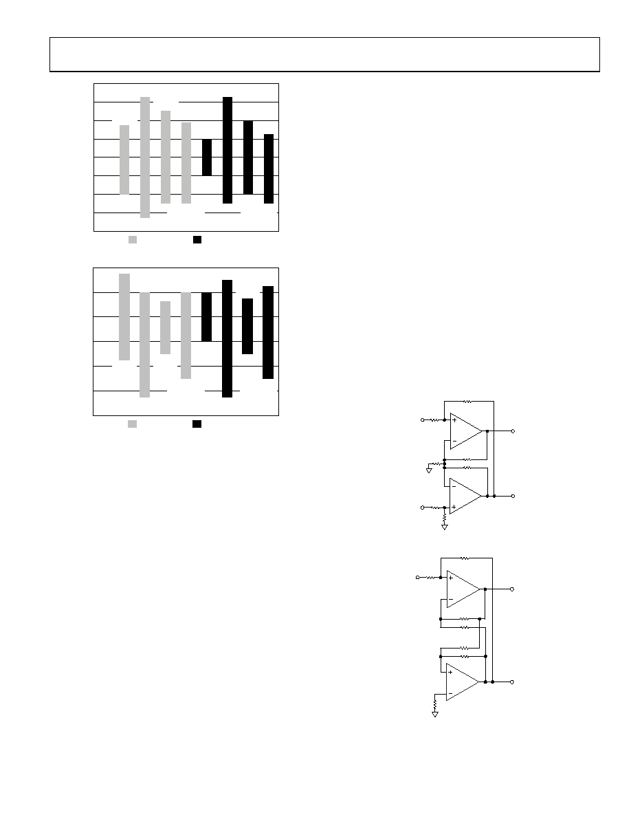
This single-ended-to-differential conversion can be performed
using an op amp pair. Typical connection diagrams for an op
amp pair are shown in Figure 42 and Figure 43. In Figure 42,
the common-mode signal is applied to the noninverting input
of the second amplifier.
VIN
V+
V–
3k
1.5k
1.5k
1.5k
1.5k
10k
20k
VCOM
05401-
029
AD845
Figure 42. Single-Ended-to-Differential Configuration with the AD845
VIN
V+
V–
442
442
442
442
442
100
AD8021
442
05401-
030
Figure 43. Single-Ended-to-Differential Configuration with the AD8021
相关PDF资料 |
PDF描述 |
|---|---|
| AD790JRZ-REEL7 | IC COMPARATOR PREC W/LATCH 8SOIC |
| AD7888ARUZ | IC ADC 12BIT 8CH SRL 16-TSSOP |
| 1676855-3 | CAP CER 0.68PF 100V 5% NP0 0603 |
| AD7949BCPZ | IC ADC 14BIT 250KSPS 8CH 20LFCSP |
| 1676855-2 | CAP CER 0.56PF 100V 5% NP0 0603 |
相关代理商/技术参数 |
参数描述 |
|---|---|
| AD7327BRUZ-REEL | 功能描述:IC ADC 12BIT+SAR 8CHAN 20-TSSOP RoHS:是 类别:集成电路 (IC) >> 数据采集 - 模数转换器 系列:- 标准包装:1,000 系列:- 位数:16 采样率(每秒):45k 数据接口:串行 转换器数目:2 功率耗散(最大):315mW 电压电源:模拟和数字 工作温度:0°C ~ 70°C 安装类型:表面贴装 封装/外壳:28-SOIC(0.295",7.50mm 宽) 供应商设备封装:28-SOIC W 包装:带卷 (TR) 输入数目和类型:2 个单端,单极 |
| AD7327BRUZ-REEL7 | 功能描述:IC ADC 12BIT+ SAR 8CHAN 20TSSOP RoHS:是 类别:集成电路 (IC) >> 数据采集 - 模数转换器 系列:- 标准包装:1,000 系列:- 位数:16 采样率(每秒):45k 数据接口:串行 转换器数目:2 功率耗散(最大):315mW 电压电源:模拟和数字 工作温度:0°C ~ 70°C 安装类型:表面贴装 封装/外壳:28-SOIC(0.295",7.50mm 宽) 供应商设备封装:28-SOIC W 包装:带卷 (TR) 输入数目和类型:2 个单端,单极 |
| AD7328 | 制造商:AD 制造商全称:Analog Devices 功能描述:8-Channel, Software-Selectable True Bipolar Input, 12-Bit Plus Sign ADC |
| AD7328BRUZ | 功能描述:IC ADC 12BIT+ SAR 8CHAN 20TSSOP RoHS:是 类别:集成电路 (IC) >> 数据采集 - 模数转换器 系列:iCMOS® 标准包装:1 系列:microPOWER™ 位数:8 采样率(每秒):1M 数据接口:串行,SPI? 转换器数目:1 功率耗散(最大):- 电压电源:模拟和数字 工作温度:-40°C ~ 125°C 安装类型:表面贴装 封装/外壳:24-VFQFN 裸露焊盘 供应商设备封装:24-VQFN 裸露焊盘(4x4) 包装:Digi-Reel® 输入数目和类型:8 个单端,单极 产品目录页面:892 (CN2011-ZH PDF) 其它名称:296-25851-6 |
| AD7328BRUZ | 制造商:Analog Devices 功能描述:A/D Converter (A-D) IC |
发布紧急采购,3分钟左右您将得到回复。