- 您现在的位置:买卖IC网 > PDF目录373897 > AD73311LARS (ANALOG DEVICES INC) Low Cost, Low Power CMOS General Purpose Analog Front End PDF资料下载
参数资料
| 型号: | AD73311LARS |
| 厂商: | ANALOG DEVICES INC |
| 元件分类: | 通信及网络 |
| 英文描述: | Low Cost, Low Power CMOS General Purpose Analog Front End |
| 中文描述: | SPECIALTY TELECOM CIRCUIT, PDSO20 |
| 封装: | SSOP-20 |
| 文件页数: | 12/36页 |
| 文件大小: | 382K |
| 代理商: | AD73311LARS |
第1页第2页第3页第4页第5页第6页第7页第8页第9页第10页第11页当前第12页第13页第14页第15页第16页第17页第18页第19页第20页第21页第22页第23页第24页第25页第26页第27页第28页第29页第30页第31页第32页第33页第34页第35页第36页
REV. A
AD73311L
–12–
SPORT Register Maps
There are two register banks for the AD73311L: the control
register bank and the data register bank. The control register
bank consists of six read/write registers, each eight bits wide.
Table IX shows the control register map for the AD73311L.
The
fi
rst two control registers, CRA and CRB, are reserved for
controlling the SPORT. They hold settings for parameters such
as bit rate, internal master clock rate and device count (used
when more than one AD73311L is connected in cascade from
a single SPORT). The other three registers; CRC, CRD and
CRE are used to hold control settings for the ADC, DAC,
Reference and Power Control sections of the device. Control
registers are written to on the negative edge of SCLK. The
data register bank consists of two 16-bit registers that are the
DAC and ADC registers.
Master Clock Divider
The AD73311L features a programmable master clock divider
that allows the user to reduce an externally available master
clock, at pin MCLK, by one of the ratios 1, 2, 3, 4 or 5 to
produce an internal master clock signal (DMCLK) that is used
to calculate the sampling and serial clock rates. The master
clock divider is programmable by setting CRB:4-6. Table V shows
the division ratio corresponding to the various bit settings. The
default divider ratio is divide-by-one.
Table V. DMCLK (Internal) Rate Divider Settings
MCD2
MCD1
MCD0
DMCLK Rate
0
0
0
0
1
1
1
1
0
0
1
1
0
0
1
1
0
1
0
1
0
1
0
1
MCLK
MCLK/2
MCLK/3
MCLK/4
MCLK/5
MCLK
MCLK
MCLK
Serial Clock Rate Divider
The AD73311L features a programmable serial clock divider that
allows users to match the serial clock (SCLK) rate of the data to
that of the DSP engine or host processor. The maximum SCLK
rate available is DMCLK and the other available rates are:
DMCLK/2, DMCLK/4 and DMCLK/8. The slowest rate
(DMCLK/8) is the default SCLK rate. The serial clock divider
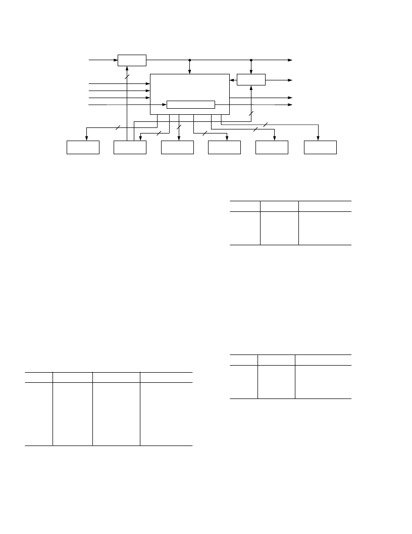
Figure 9. SPORT Block Diagram
is programmable by setting bits CRB:2
–
3. Table VI shows the
serial clock rate corresponding to the various bit settings.
Table VI. SCLK Rate Divider Settings
SCD1
SCD0
SCLK Rate
0
0
1
1
0
1
0
1
DMCLK/8
DMCLK/4
DMCLK/2
DMCLK
Sample Rate Divider
The AD73311L features a programmable sample rate divider
that allows users flexibility in matching the codec
’
s ADC and
DAC sample rates to the needs of the DSP software. The maxi-
mum sample rate available is DMCLK/256 which offers the
lowest conversion group delay, while the other available rates
are: DMCLK/512, DMCLK/1024 and DMCLK/2048. The
slowest rate (DMCLK/2048) is the default sample rate. The
sample rate divider is programmable by setting bits CRB:0-1.
Table VII shows the sample rate corresponding to the various
bit settings.
Table VII. Sample Rate Divider Settings
DIR1
DIR0
SCLK Rate
0
0
1
1
0
1
0
1
DMCLK/2048
DMCLK/1024
DMCLK/512
DMCLK/256
DAC Advance Register
The loading of the DAC is internally synchronized with the
unloading of the ADC data in each sampling interval. The
default DAC load event happens one SCLK cycle before the
SDOFS flag is raised by the ADC data being ready. However,
this DAC load position can be advanced before this time by
modifying the contents of the DAC Advance
fi
eld in Control
Register E (CRE:0
–
4). The
fi
eld is
fi
ve bits wide, allowing 31
increments of weight 1/(DMCLK/8); see Table VIII. In certain
circumstances this can reduce the group delay when the ADC
and DAC are used to process data in series. Appendix E details
how the DAC advance feature can be used.
NOTE: The DAC advance register should be changed before
the DAC section is powered up.
SE(SPORT)
SERIAL REGISTER
DSCLK
MCLK
CONTROL
CONTROL
CONTROL
CONTROL
CONTROL
MCLK
SE
RESET
SDIFS
SDI
DMCLK
3
8
8
8
8
8
2
SCLK
SDOFS
SDO
CONTROL
8
相关PDF资料 |
PDF描述 |
|---|---|
| AD73311LARU | Low Cost, Low Power CMOS General Purpose Analog Front End |
| AD73311AR | Low Cost, Low Power CMOS General Purpose Analog Front End |
| AD73311ARS | Low Cost, Low Power CMOS General Purpose Analog Front End |
| AD73311LAR | Low Cost, Low Power CMOS General Purpose Analog Front End |
| AD73311L | Low Cost, Low Power CMOS General Purpose Analog Front End Processor(低成本,低功耗的CMOS通用双模拟前端处理器) |
相关代理商/技术参数 |
参数描述 |
|---|---|
| AD73311LARS-REEL | 制造商:Analog Devices 功能描述:Audio Codec 1ADC / 1DAC 16-Bit 20-Pin SSOP T/R |
| AD73311LARSREEL7 | 制造商:AD 功能描述:New |
| AD73311LARS-REEL7 | 制造商:Analog Devices 功能描述:Audio Codec 1ADC / 1DAC 16-Bit 20-Pin SSOP T/R |
| AD73311LARSZ | 功能描述:IC PROCESSOR FRONT END LP 20SSOP RoHS:是 类别:集成电路 (IC) >> 数据采集 - 模拟前端 (AFE) 系列:- 产品培训模块:Lead (SnPb) Finish for COTS Obsolescence Mitigation Program 标准包装:2,500 系列:- 位数:- 通道数:2 功率(瓦特):- 电压 - 电源,模拟:3 V ~ 3.6 V 电压 - 电源,数字:3 V ~ 3.6 V 封装/外壳:32-VFQFN 裸露焊盘 供应商设备封装:32-QFN(5x5) 包装:带卷 (TR) |
| AD73311LARSZ-REEL | 功能描述:IC PROCESSOR FRONT END LP 20SSOP RoHS:是 类别:集成电路 (IC) >> 数据采集 - 模拟前端 (AFE) 系列:- 产品培训模块:Lead (SnPb) Finish for COTS Obsolescence Mitigation Program 标准包装:2,500 系列:- 位数:- 通道数:2 功率(瓦特):- 电压 - 电源,模拟:3 V ~ 3.6 V 电压 - 电源,数字:3 V ~ 3.6 V 封装/外壳:32-VFQFN 裸露焊盘 供应商设备封装:32-QFN(5x5) 包装:带卷 (TR) |
发布紧急采购,3分钟左右您将得到回复。