- 您现在的位置:买卖IC网 > PDF目录10786 > AD7391ANZ (Analog Devices Inc)IC DAC 10BIT SERIAL 3V 8-DIP PDF资料下载
参数资料
| 型号: | AD7391ANZ |
| 厂商: | Analog Devices Inc |
| 文件页数: | 11/12页 |
| 文件大小: | 0K |
| 描述: | IC DAC 10BIT SERIAL 3V 8-DIP |
| 产品培训模块: | Data Converter Fundamentals DAC Architectures |
| 产品变化通告: | Product Discontinuance 27/Oct/2011 |
| 标准包装: | 50 |
| 设置时间: | 70µs |
| 位数: | 10 |
| 数据接口: | 串行,SPI? |
| 转换器数目: | 1 |
| 电压电源: | 单电源 |
| 功率耗散(最大): | 500µW |
| 工作温度: | -40°C ~ 85°C |
| 安装类型: | 通孔 |
| 封装/外壳: | 8-DIP(0.300",7.62mm) |
| 供应商设备封装: | 8-PDIP |
| 包装: | 管件 |
| 输出数目和类型: | 1 电压,单极;1 电压,双极 |
| 采样率(每秒): | 17k |
REV. A
AD7390/AD7391
–8–
OPERATION
The AD7390 and AD7391 are a set of pin compatible, 12-bit/
10-bit digital-to-analog converters. These single-supply opera-
tion devices consume less than 100 microamps of current while
operating from power supplies in the 2.7 V to 5.5 V range mak-
ing them ideal for battery operated applications. They contain a
voltage-switched, 12-bit/10-bit, laser-trimmed digital-to-analog
converter, rail-to-rail output op amps, serial-input register, and
a DAC register. The external reference input has constant input
resistance independent of the digital code setting of the DAC.
In addition, the reference input can be tied to the same supply
voltage as VDD resulting in a maximum output voltage span of
0 to VDD. The SPI compatible, serial-data interface consists of
a serial data input (SDI), clock (CLK), and load (
LD) pins.
A
CLR pin is available to reset the DAC register to zero-scale.
This function is useful for power-on reset or system failure
recovery to a known state.
D/A CONVERTER SECTION
The voltage switched R-2R DAC generates an output voltage
dependent on the external reference voltage connected to the
VREF pin according to the following equation:
VV
D
OUT
REF
N
=×
2
(1)
where D is the decimal data word loaded into the DAC register,
and N is the number of bits of DAC resolution. In the case of the
10-bit AD7391 using a 2.5 V reference, Equation 1 simplifies to:
V
D
OUT
=×
25
1024
.
(2)
Using Equation 2 the nominal midscale voltage at VOUT is
1.25 V for D = 512; full-scale voltage is 2.497 V. The LSB step
size is = 2.5
1/1024 = 0.0024 V.
For the 12-bit AD7390 operating from a 5.0 V reference
Equation 1 becomes:
V
D
OUT
=×
50
4096
.
(3)
Using Equation 3 the AD7390 provides a nominal midscale
voltage of 2.5 V for D = 2048, and a full-scale output of 4.998 V.
The LSB step size is = 5.0
1/4096 = 0.0012 V.
AMPLIFIER SECTION
The internal DAC’s output is buffered by a low power con-
sumption precision amplifier. The op amp has a 60
s typical
settling time to 0.1% of full scale. There are slight differences in
settling time for negative slewing signals versus positive. Also,
negative transition settling time to within the last 6 LSBs of zero
volts has an extended settling time. The rail-to-rail output stage
of this amplifier has been designed to provide precision perfor-
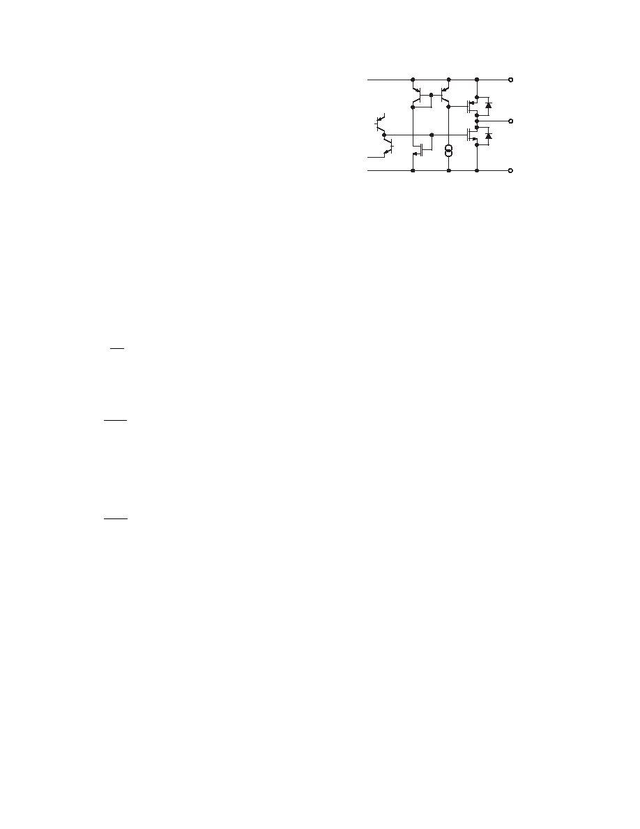
mance while operating near either power supply. Figure 5
shows an equivalent output schematic of the rail-to-rail ampli-
fier with its N-channel pull-down FETs that will pull an output
load directly to GND. The output sourcing current is provided
by a P-channel pull-up device that can source current to GND
terminated loads.
AGND
VOUT
VDD
P-CH
N-CH
Figure 5. Equivalent Analog Output Circuit
The rail-to-rail output stage provides
±1 mA of output current.
The N-channel output pull-down MOSFET shown in Figure 5
has a 35
ON resistance, which sets the sink current capability
near ground. In addition to resistive load driving capability, the
amplifier has also been carefully designed and characterized for
up to 100 pF capacitive load driving capability.
REFERENCE INPUT
The reference input terminal has a constant input-resistance
independent of digital code which results in reduced glitches on
the external reference voltage source. The high 2 M
input-
resistance minimizes power dissipation within the AD7390/
AD7391 D/A converters. The VREF input accepts input voltages
ranging from ground to the positive-supply voltage VDD. One of
the simplest applications which saves an external reference
voltage source is connection of the VREF terminal to the positive
VDD supply. This connection results in a rail-to-rail voltage
output span maximizing the programmed range. The reference
input will accept ac signals as long as they are kept within the
supply voltage range, 0 < VREF IN < VDD. The reference band-
width and integral nonlinearity error performance are plotted in
the typical performance section (see TPCs 14 and 15). The
ratiometric reference feature makes the AD7390/AD7391 an
ideal companion to ratiometric analog-to-digital converters such
as the AD7896.
POWER SUPPLY
The very low power consumption of the AD7390/AD7391 is a
direct result of a circuit design optimizing the use of a CBCMOS
process. By using the low power characteristics of CMOS for the
logic, and the low noise, tight-matching of the complementary
bipolar transistors, excellent analog accuracy is achieved. One
advantage of the rail-to-rail output amplifiers used in the AD7390/
AD7391 is the wide range of usable supply voltage. The part is
fully specified and tested for operation from 2.7 V to 5.5 V.
POWER SUPPLY BYPASSING AND GROUNDING
Precision analog products, such as the AD7390/AD7391, require
a well filtered power source. Since the AD7390/AD7391 operates
from a single 3 V to 5 V supply, it seems convenient to simply tap
into the digital logic power supply. Unfortunately, the logic sup-
ply is often a switch-mode design, which generates noise in the
20 kHz to 1 MHz range. In addition, fast logic gates can generate
glitches hundred of millivolts in amplitude due to wiring resis-
tance and inductance. The power supply noise generated thereby
means that special care must be taken to assure that the inherent
precision of the DAC is maintained. Good engineering judgment
should be exercised when addressing the power supply ground-
ing and bypassing of the AD7390.
相关PDF资料 |
PDF描述 |
|---|---|
| AD7541AJPZ | IC DAC 12BIT MULT MONO 20PLCC |
| AD7111ACRZ | IC DAC MONO MULTIPLYING 16SOIC |
| AD7111ACNZ | IC DAC MONO MULTIPLYING 16-DIP |
| AD7111ABRZ | IC DAC MONO MULTIPLYING 16SOIC |
| AD7808BNZ | IC DAC 10BIT OCTAL SERIAL 24DIP |
相关代理商/技术参数 |
参数描述 |
|---|---|
| AD7391AR | 功能描述:IC DAC 10BIT 3V SRL-IN 8-SOIC RoHS:否 类别:集成电路 (IC) >> 数据采集 - 数模转换器 系列:- 标准包装:47 系列:- 设置时间:2µs 位数:14 数据接口:并联 转换器数目:1 电压电源:单电源 功率耗散(最大):55µW 工作温度:-40°C ~ 85°C 安装类型:表面贴装 封装/外壳:28-SSOP(0.209",5.30mm 宽) 供应商设备封装:28-SSOP 包装:管件 输出数目和类型:1 电流,单极;1 电流,双极 采样率(每秒):* |
| AD7391AR-REEL | 功能描述:IC DAC 10BIT SRL 3V 8-SOIC T/R RoHS:否 类别:集成电路 (IC) >> 数据采集 - 数模转换器 系列:- 产品培训模块:LTC263x 12-, 10-, and 8-Bit VOUT DAC Family 特色产品:LTC2636 - Octal 12-/10-/8-Bit SPI VOUT DACs with 10ppm/°C Reference 标准包装:91 系列:- 设置时间:4µs 位数:10 数据接口:MICROWIRE?,串行,SPI? 转换器数目:8 电压电源:单电源 功率耗散(最大):2.7mW 工作温度:-40°C ~ 85°C 安装类型:表面贴装 封装/外壳:14-WFDFN 裸露焊盘 供应商设备封装:14-DFN-EP(4x3) 包装:管件 输出数目和类型:8 电压,单极 采样率(每秒):* |
| AD7391AR-REEL7 | 功能描述:IC DAC 10BIT SRL 3V 8-SOIC T/R RoHS:否 类别:集成电路 (IC) >> 数据采集 - 数模转换器 系列:- 产品培训模块:LTC263x 12-, 10-, and 8-Bit VOUT DAC Family 特色产品:LTC2636 - Octal 12-/10-/8-Bit SPI VOUT DACs with 10ppm/°C Reference 标准包装:91 系列:- 设置时间:4µs 位数:10 数据接口:MICROWIRE?,串行,SPI? 转换器数目:8 电压电源:单电源 功率耗散(最大):2.7mW 工作温度:-40°C ~ 85°C 安装类型:表面贴装 封装/外壳:14-WFDFN 裸露焊盘 供应商设备封装:14-DFN-EP(4x3) 包装:管件 输出数目和类型:8 电压,单极 采样率(每秒):* |
| AD7391ARU | 功能描述:IC DAC 10BIT SRL 3V 8-TSSOP RoHS:否 类别:集成电路 (IC) >> 数据采集 - 数模转换器 系列:- 标准包装:2,400 系列:- 设置时间:- 位数:18 数据接口:串行 转换器数目:3 电压电源:模拟和数字 功率耗散(最大):- 工作温度:-40°C ~ 85°C 安装类型:表面贴装 封装/外壳:36-TFBGA 供应商设备封装:36-TFBGA 包装:带卷 (TR) 输出数目和类型:* 采样率(每秒):* |
| AD7391ARU-REEL | 功能描述:IC DAC 10BIT SRL 3V 8-TSSOP T/R RoHS:否 类别:集成电路 (IC) >> 数据采集 - 数模转换器 系列:- 产品培训模块:LTC263x 12-, 10-, and 8-Bit VOUT DAC Family 特色产品:LTC2636 - Octal 12-/10-/8-Bit SPI VOUT DACs with 10ppm/°C Reference 标准包装:91 系列:- 设置时间:4µs 位数:10 数据接口:MICROWIRE?,串行,SPI? 转换器数目:8 电压电源:单电源 功率耗散(最大):2.7mW 工作温度:-40°C ~ 85°C 安装类型:表面贴装 封装/外壳:14-WFDFN 裸露焊盘 供应商设备封装:14-DFN-EP(4x3) 包装:管件 输出数目和类型:8 电压,单极 采样率(每秒):* |
发布紧急采购,3分钟左右您将得到回复。