参数资料
| 型号: | AD7391ARUZ |
| 厂商: | Analog Devices Inc |
| 文件页数: | 12/12页 |
| 文件大小: | 0K |
| 描述: | IC DAC 10BIT SRL 8TSSOP |
| 标准包装: | 96 |
| 设置时间: | 70µs |
| 位数: | 10 |
| 数据接口: | 串行,SPI? |
| 转换器数目: | 1 |
| 电压电源: | 单电源 |
| 功率耗散(最大): | 500µW |
| 工作温度: | -40°C ~ 85°C |
| 安装类型: | 表面贴装 |
| 封装/外壳: | 8-TSSOP(0.173",4.40mm 宽) |
| 供应商设备封装: | 8-TSSOP |
| 包装: | 管件 |
| 输出数目和类型: | 1 电压,单极;1 电压,双极 |
| 采样率(每秒): | 17k |
REV. A
AD7390/AD7391
–9–
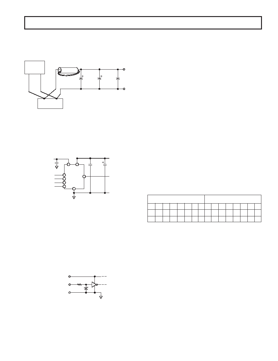
The AD7390 should be powered directly from the system
power supply. This arrangement, shown in Figure 6, employs an
LC filter and separate power and ground connections to isolate
the analog section from the logic switching transients.
FERRITE BEAD:
TWO TURNS, FAIR-RITE
#2677006301
TTL/CMOS
LOGIC
CIRCUITS
5V
POWER SUPPLY
100 F
ELECT.
10 F–22 F
TANTALUM
0.1 F
CERAMIC
CAPACITOR
5V
RETURN
Figure 6. Use Separate Traces to Reduce Power
Supply Noise
Whether or not a separate power supply trace is available, how-
ever, generous supply bypassing will reduce supply-line induced
errors. Local supply bypassing consisting of a 10
F tantalum
electrolytic in parallel with a 0.1
F ceramic capacitor is recom-
mended in all applications (Figure 7).
AD7390
OR
AD7391
0.1 F
CLK
VOUT
REF
VDD
GND
C
*
10 F
6
7
8
5
1
2
3
4
SDI
CLR
LD
*OPTIONAL EXTERNAL
REFERENCE BYPASS
2.7V TO 5.5V
Figure 7. Recommended Supply Bypassing
INPUT LOGIC LEVELS
All digital inputs are protected with a Zener-type ESD protection
structure (Figure 8) that allows logic input voltages to exceed the
VDD supply voltage. This feature can be useful if the user is driving
one or more of the digital inputs with a 5 V CMOS logic input-
voltage level while operating the AD7390/AD7391 on a 3 V power
supply. If this mode of interface is used, make sure that the VOL
of the 5 V CMOS meets the VIL input requirement of the AD7390/
AD7391 operating at 3 V. See TPC 6 for a graph for digital
logic input threshold versus operating VDD supply voltage.
LOGIC
IN
VDD
GND
Figure 8. Equivalent Digital Input ESD Protection
In order to minimize power dissipation from input-logic levels that
are near the VIH and VIL logic input voltage specifications, a
Schmitt trigger design was used that minimizes the input-buffer
current consumption compared to traditional CMOS input
stages. TPC 5 shows a plot of incremental input voltage versus
supply current showing that negligible current consumption
takes place when logic levels are in their quiescent state. The
normal crossover current still occurs during logic transitions. A
secondary advantage of this Schmitt trigger is the prevention of
false triggers that would occur with slow moving logic transi-
tions when a standard CMOS logic interface or opto isolators
are used. The logic inputs SDI, CLK,
LD, CLR all contain the
Schmitt trigger circuits.
DIGITAL INTERFACE
The AD7390/AD7391 have a double-buffered serial data input.
The serial-input register is separate from the DAC register,
which allows preloading of a new data value into the serial regis-
ter without disturbing the present DAC values. A functional
block diagram of the digital section is shown in Figure 4, while
Table I contains the truth table for the control logic inputs.
Three pins control the serial data input. Data at the Serial Data
Input (SDI) is clocked into the shift register on the rising edge
of CLK. Data is entered in MSB-first format. Twelve clock
pulses are required to load the 12-bit AD7390 DAC value. If
additional bits are clocked into the shift register, for example
when a microcontroller sends two 8-bit bytes, the MSBs are
ignored (Figure 9). The CLK pin is only enabled when Load
(
LD) is high. The lower resolution 10-bit AD7391 contains a
10-bit shift register. The AD7391 is also loaded MSB first with
10 bits of data. Again if additional bits are clocked into the shift
register, only the last 10 bits clocked in are used.
The Load pin (
LD) controls the flow of data from the shift
register to the DAC register. After a new value is clocked into
the serial-input register, it will be transferred to the DAC register
by the negative transition of the Load pin (
LD).
BYTE 1
BYTE 0
MSB
LSB
MSB
LSB
B15 B14 B13 B12 B11 B10 B9
B8
B7
B6
B5
B4
B3
B2
B1
B0
X
D11 D10 D9
D8
D7
D6
D5
D4
D3
D2
D1
D0
X
D9
D8
D7
D6
D5
D4
D3
D2
D1
D0
D11–D0: 12-BIT AD7390 DAC VALUE; D9–D0: 10-BIT AD7391 DAC VALUE
X = DON’T CARE
THE MSB OF BYTE 1 IS THE FIRST BIT THAT IS LOADED INTO THE DAC
Figure 9. Typical AD7390-Microprocessor Serial Data
Input Forms
RESET (
CLR) PIN
Forcing the
CLR pin low will set the DAC register to all zeros
and the DAC output voltage will be zero volts. The reset function
is useful for setting the DAC outputs to zero at power-up or
after a power supply interruption. Test systems and motor
controllers are two of many applications which benefit from
powering up to a known state. The external reset pulse can be
generated by the microprocessor’s power-on RESET signal, by
an output from the microprocessor, or by an external resistor
and capacitor.
CLR has a Schmitt trigger input which results in
a clean reset function when using external resistor/capacitor
generated pulses. The
CLR input overrides other logic inputs,
specifically
LD. However, LD should be set high before CLR
goes high. If
CLR is kept low, then the contents of the shift
register will be transferred to the DAC register as soon as
CLR
returns high. See the Control-Logic Truth Table I.
相关PDF资料 |
PDF描述 |
|---|---|
| SY100EL11VZI TR | IC CLOCK FANOUT BUFFER 1:2 8SOIC |
| VI-J4J-MY | CONVERTER MOD DC/DC 36V 50W |
| SY100E310LJI | IC CLOCK BUFFER MUX 2:8 28-PLCC |
| LTC1450CG | IC D/A CONV 12BIT R-R PAR 24SSOP |
| LTC1658IS8#PBF | IC D/A CONV 14BIT R-R 8-SOIC |
相关代理商/技术参数 |
参数描述 |
|---|---|
| AD7391ARUZ-REEL | 功能描述:IC DAC 10BIT SRL 8TSSOP RoHS:是 类别:集成电路 (IC) >> 数据采集 - 数模转换器 系列:- 产品培训模块:LTC263x 12-, 10-, and 8-Bit VOUT DAC Family 特色产品:LTC2636 - Octal 12-/10-/8-Bit SPI VOUT DACs with 10ppm/°C Reference 标准包装:91 系列:- 设置时间:4µs 位数:10 数据接口:MICROWIRE?,串行,SPI? 转换器数目:8 电压电源:单电源 功率耗散(最大):2.7mW 工作温度:-40°C ~ 85°C 安装类型:表面贴装 封装/外壳:14-WFDFN 裸露焊盘 供应商设备封装:14-DFN-EP(4x3) 包装:管件 输出数目和类型:8 电压,单极 采样率(每秒):* |
| AD7391ARZ | 功能描述:IC DAC 10BIT 3V SRL-IN 8-SOIC RoHS:是 类别:集成电路 (IC) >> 数据采集 - 数模转换器 系列:- 产品培训模块:Lead (SnPb) Finish for COTS Obsolescence Mitigation Program 标准包装:50 系列:- 设置时间:4µs 位数:12 数据接口:串行 转换器数目:2 电压电源:单电源 功率耗散(最大):- 工作温度:-40°C ~ 85°C 安装类型:表面贴装 封装/外壳:8-TSSOP,8-MSOP(0.118",3.00mm 宽) 供应商设备封装:8-uMAX 包装:管件 输出数目和类型:2 电压,单极 采样率(每秒):* 产品目录页面:1398 (CN2011-ZH PDF) |
| AD7391ARZ | 制造商:Analog Devices 功能描述:IC 10-BIT MICROPOWER DAC |
| AD7391ARZ-REEL | 功能描述:IC DAC 10BIT 3V SRL-IN 8-SOIC RoHS:是 类别:集成电路 (IC) >> 数据采集 - 数模转换器 系列:- 产品培训模块:LTC263x 12-, 10-, and 8-Bit VOUT DAC Family 特色产品:LTC2636 - Octal 12-/10-/8-Bit SPI VOUT DACs with 10ppm/°C Reference 标准包装:91 系列:- 设置时间:4µs 位数:10 数据接口:MICROWIRE?,串行,SPI? 转换器数目:8 电压电源:单电源 功率耗散(最大):2.7mW 工作温度:-40°C ~ 85°C 安装类型:表面贴装 封装/外壳:14-WFDFN 裸露焊盘 供应商设备封装:14-DFN-EP(4x3) 包装:管件 输出数目和类型:8 电压,单极 采样率(每秒):* |
| AD7391ARZ-REEL7 | 功能描述:IC DAC 10BIT 3V SRL-IN 8-SOIC RoHS:是 类别:集成电路 (IC) >> 数据采集 - 数模转换器 系列:- 产品培训模块:LTC263x 12-, 10-, and 8-Bit VOUT DAC Family 特色产品:LTC2636 - Octal 12-/10-/8-Bit SPI VOUT DACs with 10ppm/°C Reference 标准包装:91 系列:- 设置时间:4µs 位数:10 数据接口:MICROWIRE?,串行,SPI? 转换器数目:8 电压电源:单电源 功率耗散(最大):2.7mW 工作温度:-40°C ~ 85°C 安装类型:表面贴装 封装/外壳:14-WFDFN 裸露焊盘 供应商设备封装:14-DFN-EP(4x3) 包装:管件 输出数目和类型:8 电压,单极 采样率(每秒):* |
发布紧急采购,3分钟左右您将得到回复。