- 您现在的位置:买卖IC网 > PDF目录8661 > AD7396ARZ-REEL (Analog Devices Inc)IC DAC 12BIT PARALLEL 3V 24-SOIC PDF资料下载
参数资料
| 型号: | AD7396ARZ-REEL |
| 厂商: | Analog Devices Inc |
| 文件页数: | 12/12页 |
| 文件大小: | 0K |
| 描述: | IC DAC 12BIT PARALLEL 3V 24-SOIC |
| 产品培训模块: | Data Converter Fundamentals DAC Architectures |
| 标准包装: | 1,000 |
| 设置时间: | 60µs |
| 位数: | 12 |
| 数据接口: | 并联 |
| 转换器数目: | 2 |
| 电压电源: | 单电源 |
| 功率耗散(最大): | 1mW |
| 工作温度: | -40°C ~ 85°C |
| 安装类型: | 表面贴装 |
| 封装/外壳: | 24-SOIC(0.295",7.50mm 宽) |
| 供应商设备封装: | 24-SOIC W |
| 包装: | 带卷 (TR) |
| 输出数目和类型: | 2 电压,单极;2 电压,双极 |
| 采样率(每秒): | 17k |
AD7396/AD7397
–9–
REV. 0
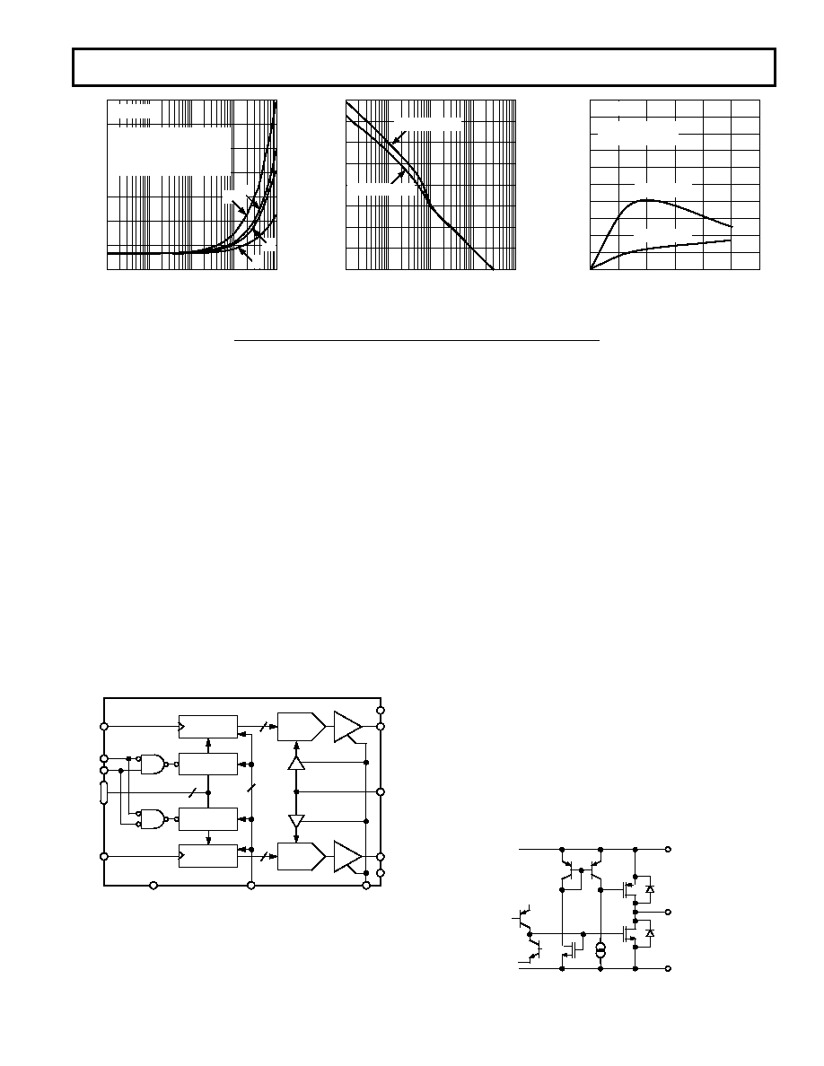
DIGITAL INPUT FREQUENCY – Hz
I DD
–
A
1400
1k
10M
10k
100k
1M
1200
1000
800
600
400
200
0
AD7396
A: VDD = +2.7V, CODE = 555H
B: VDD = +2.7V, CODE = 3FFH
C: VDD = +5.5V, CODE = 155H
D: VDD = +5.5V, CODE = 3FFH
D
C
B
A
Figure 22. IDD vs. Digital Input
Frequency
OPERATION
The AD7396 and AD7397 are a set of pin compatible, 12-bit
and 10-bit digital-to-analog converters. These single-supply
operation devices consume less than 200
A of current while
operating from power supplies in the +2.7 V to +5.5 V range,
making them ideal for battery operated applications. They
contain a voltage-switched, 12-bit/10-bit, digital-to-analog
converter, rail-to-rail output op amps, and a parallel-input
DAC register. The external reference input has constant
2.5 M
input resistance independent of the digital code
setting of the DAC. In addition, the reference input can be tied
to the same supply voltage as VDD resulting in a maximum
output voltage span of 0 to VDD. The parallel data interface
consists of 12 data bits, DB0–DB11, for the AD7396, 10 data
bits, DB0–DB9, for the AD7397, and a
CS write strobe. An RS
pin is available to reset the DAC register to zero scale. This
function is useful for power-on reset or system failure recovery
to a known state. Additional power savings are accomplished by
activating the
SHDN pin resulting in a 1.5
A maximum con-
sumption sleep mode. As long as the supply voltage, remains
data will be retained in the DAC and input register to supply
the DAC output when the part is taken out of shutdown.
DACA
REGISTER
12
INPUTA
REGISTER
DACB
REGISTER
12
INPUTB
REGISTER
AD7396
12-BIT
DACA
12-BIT
DACB
1
DATA
LDA
CS
A/
B
DGND
RS
SHDN
VDD
VOUTA
VREF
VOUTB
AGND
LDB
12
Figure 25. Functional Block Diagram
D/A CONVERTER SECTION
The voltage switched R-2R DAC generates an output voltage
dependent on the external reference voltage connected to the
REF pin according to the following equation:
VOUT = VREF
× D/2N
(1)
where D is the decimal data word loaded into the DAC register,
and N is the number of bits of DAC resolution. In the case of
the 10-bit AD7397 using a 2.5 V reference, Equation 1 simpli-
fies to:
VOUT = 2.5
× D/1024
(2)
Using Equation 2, the nominal midscale voltage at VOUT is
1.25 V for D = 512; full-scale voltage is 2.497 V. The LSB step
size is = 2.5
× 1/1024 = 0.0024 V.
For the 12-bit AD7396 operating from a 5.0 V reference equa-
tion [1] becomes:
VOUT = 5.0
× D/4096
(3)
Using Equation 3, the AD7396 provides a nominal midscale
voltage of 2.50 V for D = 2048, and a full-scale output of
4.998 V. The LSB step size is = 5.0
× 1/4096 = 0.0012 V.
AMPLIFIER SECTION
The internal DAC’s output is buffered by a low power con-
sumption precision amplifier. The op amp has a 60
s typical
settling time to 0.1% of full scale. There are slight differences in
settling time for negative slewing signals versus positive. Also,
negative transition settling time to within the last 6 LSBs of zero
volts has an extended settling time. The rail-to-rail output stage
of this amplifier has been designed to provide precision perfor-
mance while operating near either power supply. Figure 26
shows an equivalent output schematic of the rail-to-rail-ampli-
fier with its N-channel pull-down FETs that will pull an output
load directly to GND. The output sourcing current is provided
by a P-channel pull-up device that can source current to GND
terminated loads.
P-ch
N-ch
VDD
VOUT
AGND
Figure 26. Equivalent Analog Output Circuit
FREQUENCY – Hz
PSRR
–
dB
80
1
10k
10
100
1k
70
60
50
40
30
20
0
10
VDD = +5V, 5%
VDD = +3V, 5%
Figure 23. PSRR vs. Frequency
HOURS OF OPERATION AT +150 C
NOMINAL
CHANGE
IN
VOLTAGE
–
mV
1.0
0
0.9
0.8
0.7
0.6
0.5
0.4
0.3
0.2
0.1
0
100
200
300
400
500
600
AD7396
SAMPLE SIZE = 77
VREF = +2.5V
CODE = FFFH
CODE = 000H
Figure 24. Long-Term Drift Acceler-
ated by Burn-In
相关PDF资料 |
PDF描述 |
|---|---|
| AD9742ARUZRL7 | IC DAC 12BIT 210MSPS 28-TSSOP |
| VI-B3Z-MU-B1 | CONVERTER MOD DC/DC 2V 80W |
| VI-B3Y-MU-B1 | CONVERTER MOD DC/DC 3.3V 132W |
| VI-J1F-MY | CONVERTER MOD DC/DC 72V 50W |
| VI-J1D-MY | CONVERTER MOD DC/DC 85V 50W |
相关代理商/技术参数 |
参数描述 |
|---|---|
| AD7397 | 制造商:AD 制造商全称:Analog Devices 功能描述:3 V, Parallel Input Dual 12-Bit /10-Bit DACs |
| ad7397an | 制造商:Rochester Electronics LLC 功能描述:X2, 10-BIT, +3V UPWR DAC - Bulk 制造商:Analog Devices 功能描述: 制造商:Analog Devices 功能描述:3V,Parallel Input Dual 10-Bit DACs 制造商:Analog Devices 功能描述:3 V, Parallel Input Dual 12-Bit /10-Bit DACs |
| AD7397AR | 制造商:Analog Devices 功能描述:DAC 2-CH R-2R 10-bit 24-Pin SOIC W 制造商:Rochester Electronics LLC 功能描述:X2, 10-BIT, +3V UPWR DAC - Bulk |
| AD7397AR-REEL | 制造商:Analog Devices 功能描述:DAC 2-CH R-2R 10-bit 24-Pin SOIC W T/R |
| AD7397ARU | 制造商:Analog Devices 功能描述:DAC 2-CH R-2R 10-bit 24-Pin TSSOP 制造商:Rochester Electronics LLC 功能描述:X2, 10-BIT, +3V UPWR DAC - Bulk |
发布紧急采购,3分钟左右您将得到回复。