- 您现在的位置:买卖IC网 > PDF目录8611 > AD7398BRU-REEL7 (Analog Devices Inc)IC DAC 12BIT QUAD SRL 16-TSSOP PDF资料下载
参数资料
| 型号: | AD7398BRU-REEL7 |
| 厂商: | Analog Devices Inc |
| 文件页数: | 8/24页 |
| 文件大小: | 0K |
| 描述: | IC DAC 12BIT QUAD SRL 16-TSSOP |
| 产品培训模块: | Data Converter Fundamentals DAC Architectures |
| 标准包装: | 1,000 |
| 设置时间: | 6µs |
| 位数: | 12 |
| 数据接口: | 串行,SPI? |
| 转换器数目: | 4 |
| 电压电源: | 双 ± |
| 功率耗散(最大): | 16mW |
| 工作温度: | -40°C ~ 125°C |
| 安装类型: | 表面贴装 |
| 封装/外壳: | 16-TSSOP(0.173",4.40mm 宽) |
| 供应商设备封装: | 16-TSSOP |
| 包装: | 带卷 (TR) |
| 输出数目和类型: | 4 电压,单极 |
| 采样率(每秒): | 167k |
AD7398/AD7399
Rev. C | Page 16 of 24
POWER-ON RESET
When the VDD power supply is turned on, an internal reset
strobe forces all the input and DAC registers to the zero-code
state. The VDD power supply should have a smooth positive
ramp without drooping in order to have consistent results,
especially in the region of VDD = 1.5 V to 2.2 V. The VSS supply
has no effect on the power-on reset performance. The DAC
register data stays at zero until a valid serial register data load
takes place.
ESD Protection Circuits
All logic input pins contain back-biased ESD protection Zeners
02179-
028
GND
VDD
DIGITAL INPUTS
5k
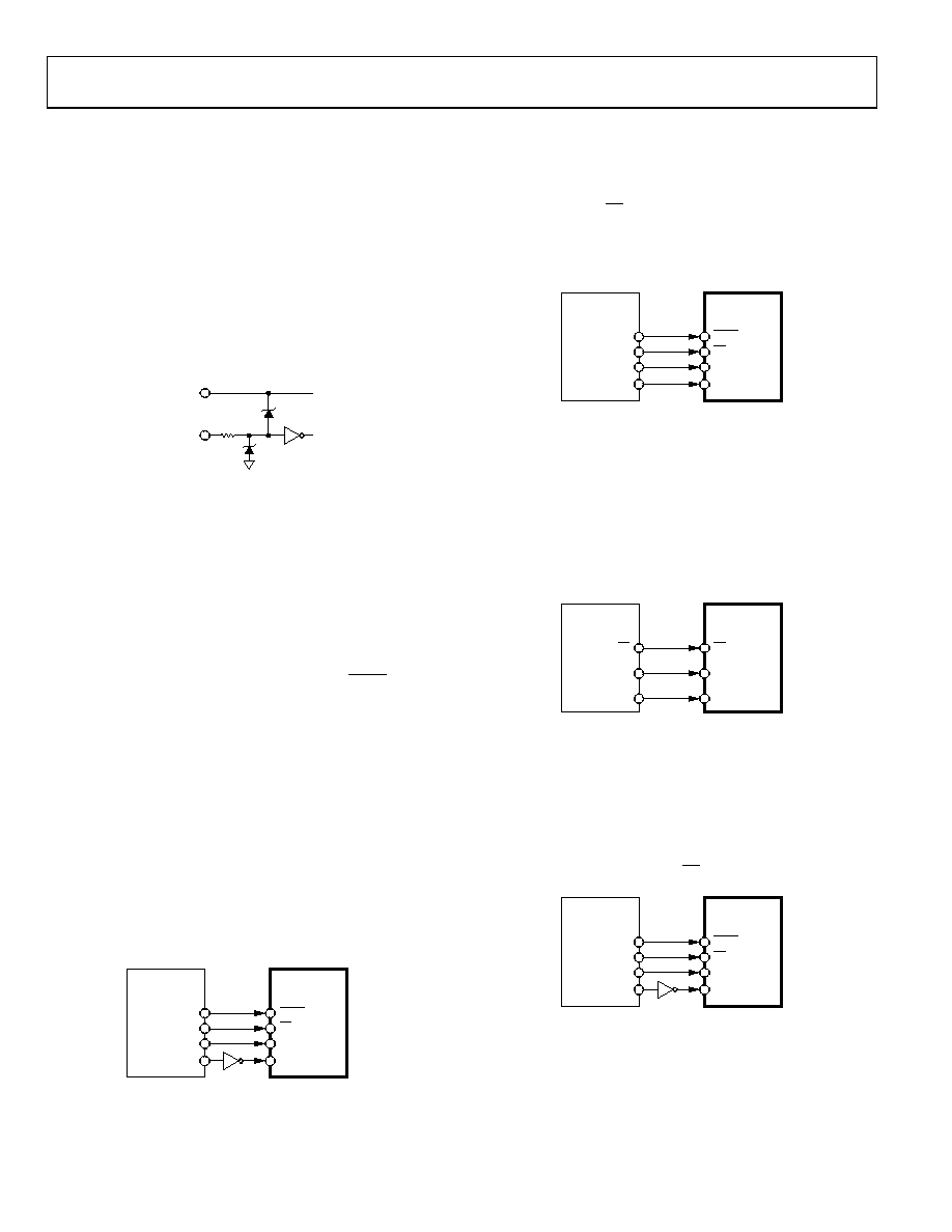
Figure 28. Equivalent ESD Protection Circuits
MICROPROCESSOR INTERFACING
Microprocessor interfacing to the AD7398/AD7399 is via a
serial bus that uses standard protocol compatible with DSP
processors and microcontrollers. The communications channel
requires a 3-wire interface consisting of a clock signal, a data
signal, and a synchronization signal. The AD7398/AD7399
require a 16-bit/14-bit data word with data valid on the rising edge
of CLK. The DAC update can be done automatically when all the
data is clocked in, or it can be done under control of LDAC.
ADSP-2101 to AD7398/AD7399 Interface
Figure 29 shows a serial interface between the AD7398/AD7399
and the ADSP-2101. The ADSP-2101 is set to operate in the serial
port (SPORT) transmit alternate framing mode. The ADSP-2101 is
programmed through the SPORT control register and should be
configured as follows: Internal clock operation, active low framing,
16-bit-word length. For the AD7398, transmission is initiated by
writing a word to the Tx register after the SPORT has been
enabled. For the AD7399, the first two bits are don’t care as the
AD7399 keeps the last 14 bits. Similarly, transmission is initiated
by writing a word to the Tx register after the SPORT has been
enabled. Because of the edge-triggered difference, an inverter is
required at the SCLKs between the DSP and the DAC.
02179-
029
AD7398/
AD7399
ADSP-21011
FO
LDAC
TFS
CS
DT
SDI
SCLK
CLK
1ADDITIONAL PINS OMITTED FOR CLARITY.
Figure 29. ADSP-2101 to AD7398/AD7399 Interface
68HC11/68L11 to AD7398/AD7399 Interface
Figure 30 shows a serial interface between the AD7398/AD7399
and the 68HC11/68L11 microcontroller. SCK of the 68HC11/
68L11 drives the CLK of the DAC, and the MOSI output drives the
serial data lines SDI. CS signal is driven from one of the port lines.
The 68HC11/68L11 are configured for master mode; MSTR = 1,
CPOL = 0, and CPHA = 0. Data appearing on the MOSI output is
valid on the rising edge of SCK.
02179-
030
AD7398/
AD7399
68HC11/
68L111
PC6
LDAC
PC7
CS
MOS1
SDI
SCK
CLK
1ADDITIONAL PINS OMITTED FOR CLARITY.
Figure 30. 68HC11/68L11 to AD7398/AD7399 Interface
MICROWIRE to AD7398/AD7399 Interface
Figure 31 shows an interface between the AD7398/AD7399 and
any MICROWIRE-compatible device. Serial data is shifted out
on the falling edge of the serial clock and into the AD7398/
AD7399 on the rising edge of the serial clock. No glue logic is
required as the DAC clocks data into the input shift register on
the rising edge.
02179-
031
AD7398/
AD7399
MICROWIRE1
SO
SDI
SCK
CLK
1ADDITIONAL PINS OMITTED FOR CLARITY.
CS
Figure 31. MICROWIRE to AD7398/AD7399 Interface
80C51/80L51 to AD7398/AD7399 Interface
A serial interface between the AD7398/AD7399 and the 80C51/
80L51 microcontroller is shown in Figure 32. TxD of the micro-
controller drives the CLK of the AD7398/AD7399, and RxD drives
the serial data line of the DAC. P3.3 is a bit-programmable pin on
the serial port that is used to drive CS.
02179-
032
AD7398/
AD7399
80C51/
80L511
P3.4
LDAC
P3.3
CS
RxD
SDI
TxD
CLK
1ADDITIONAL PINS OMITTED FOR CLARITY.
Figure 32. 80C51/80L51 to AD7398/AD7399 Interface
相关PDF资料 |
PDF描述 |
|---|---|
| ADA4937-1YCPZ-RL | IC ADC DIFF DRIVER 16-LFCSP |
| VE-24N-IV-F1 | CONVERTER MOD DC/DC 18.5V 150W |
| LTC6404IUD-4#TRPBF | IC AMP/DRIVER DIFF 16-QFN |
| VE-24M-IV-F4 | CONVERTER MOD DC/DC 10V 150W |
| VE-24M-IV-F3 | CONVERTER MOD DC/DC 10V 150W |
相关代理商/技术参数 |
参数描述 |
|---|---|
| AD7398BRUZ | 功能描述:IC DAC 12BIT QUAD SRL-IN 16TSSOP RoHS:是 类别:集成电路 (IC) >> 数据采集 - 数模转换器 系列:- 产品培训模块:Lead (SnPb) Finish for COTS Obsolescence Mitigation Program 标准包装:50 系列:- 设置时间:4µs 位数:12 数据接口:串行 转换器数目:2 电压电源:单电源 功率耗散(最大):- 工作温度:-40°C ~ 85°C 安装类型:表面贴装 封装/外壳:8-TSSOP,8-MSOP(0.118",3.00mm 宽) 供应商设备封装:8-uMAX 包装:管件 输出数目和类型:2 电压,单极 采样率(每秒):* 产品目录页面:1398 (CN2011-ZH PDF) |
| AD7398BRUZ | 制造商:Analog Devices 功能描述:IC, DAC, 12BIT, 167KSPS, TSSOP-16 |
| AD7398BRUZ-REEL7 | 功能描述:IC DAC 12BIT QUAD SERIAL 16TSSOP RoHS:是 类别:集成电路 (IC) >> 数据采集 - 数模转换器 系列:- 标准包装:47 系列:- 设置时间:2µs 位数:14 数据接口:并联 转换器数目:1 电压电源:单电源 功率耗散(最大):55µW 工作温度:-40°C ~ 85°C 安装类型:表面贴装 封装/外壳:28-SSOP(0.209",5.30mm 宽) 供应商设备封装:28-SSOP 包装:管件 输出数目和类型:1 电流,单极;1 电流,双极 采样率(每秒):* |
| AD7398BRZ | 功能描述:IC DAC 12BIT QUAD SRL 16-SOIC RoHS:是 类别:集成电路 (IC) >> 数据采集 - 数模转换器 系列:- 标准包装:1 系列:- 设置时间:4.5µs 位数:12 数据接口:串行,SPI? 转换器数目:1 电压电源:单电源 功率耗散(最大):- 工作温度:-40°C ~ 125°C 安装类型:表面贴装 封装/外壳:8-SOIC(0.154",3.90mm 宽) 供应商设备封装:8-SOICN 包装:剪切带 (CT) 输出数目和类型:1 电压,单极;1 电压,双极 采样率(每秒):* 其它名称:MCP4921T-E/SNCTMCP4921T-E/SNRCTMCP4921T-E/SNRCT-ND |
| AD7398BRZ-REEL | 功能描述:IC DAC 12BIT QUAD SERIAL 16SOIC RoHS:是 类别:集成电路 (IC) >> 数据采集 - 数模转换器 系列:- 标准包装:47 系列:- 设置时间:2µs 位数:14 数据接口:并联 转换器数目:1 电压电源:单电源 功率耗散(最大):55µW 工作温度:-40°C ~ 85°C 安装类型:表面贴装 封装/外壳:28-SSOP(0.209",5.30mm 宽) 供应商设备封装:28-SSOP 包装:管件 输出数目和类型:1 电流,单极;1 电流,双极 采样率(每秒):* |
发布紧急采购,3分钟左右您将得到回复。