- 您现在的位置:买卖IC网 > PDF目录10940 > AD74111YRUZ-REEL (Analog Devices Inc)IC CODEC AUDIO MONO LP 16TSSOP PDF资料下载
参数资料
| 型号: | AD74111YRUZ-REEL |
| 厂商: | Analog Devices Inc |
| 文件页数: | 2/20页 |
| 文件大小: | 0K |
| 描述: | IC CODEC AUDIO MONO LP 16TSSOP |
| 标准包装: | 2,500 |
| 类型: | 音频编解码器 |
| 数据接口: | 串行 |
| 分辨率(位): | 24 b |
| ADC / DAC 数量: | 1 / 1 |
| 三角积分调变: | 是 |
| S/N 比,标准 ADC / DAC (db): | 77 / 89 |
| 动态范围,标准 ADC / DAC (db): | 85 / 93 |
| 电压 - 电源,模拟: | 2.5V |
| 电压 - 电源,数字: | 2.5V |
| 工作温度: | -40°C ~ 105°C |
| 安装类型: | 表面贴装 |
| 封装/外壳: | 16-TSSOP(0.173",4.40mm 宽) |
| 供应商设备封装: | 16-TSSOP |
| 包装: | 带卷 (TR) |
REV. 0
–10–
AD74111
REFCAP
1.125V
EXTERNAL
REFERENCE
Figure 9. External Reference
Master Clocking Scheme
The update rate of the AD74111’s ADC and DAC channels
requires an internal master clock (IMCLK) that is 256 times the
sample update rate (IMCLK = 256
fS). To provide some flex-
ibility in selecting sample rates, the device has a series of three
master clock prescalers that are programmable and allow the
user to choose a range of convenient sample rates from a single
external master clock. The master clock signal to the AD74111 is
applied at the MCLK pin. The MCLK signal is passed through
a series of three programmable MCLK prescaler (divider) circuits
that can be selected to reduce the resulting Internal MCLK
(IMCLK) frequency if required. The first and second MCLK
prescalers provide divider ratios of
1 (pass through),
2,
3;
while the third prescaler provides divider ratios of
1 (pass
through),
2,
4.
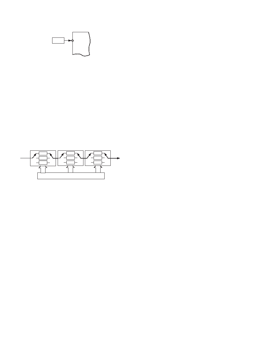
IMCLK
PROGRAMMABLE MCLK DIVIDER
CONTROL REGISTER
/1
/2
/3
/1
/2
/4
PRESCALER 2
PRESCALER 3
MCLK
/1
/2
/3
PRESCALER 1
Figure 10. MCLK Divider
The divider ratios allow a more convenient sample rate selection
from a common MCLK, which may be required in many voice
related applications. Control Register B should be programmed
to achieve the desired divider ratios.
Selecting Sample Rates
The sample rate at which the converter runs is always 256 times
the IMCLK rate. IMCLK is the Internal Master Clock and is the
output from the Master Clock Prescaler. The default sample rate
is 48 kHz (based on an external MCLK of 12.288 MHz). In this
mode, the ADC modulator is clocked at 3.072 MHz and the DAC
modulator is clocked at 6.144 MHz. Sample rates that are lower
than MCLK/256 can be achieved by using the MCLK prescaler.
Example 1: fSAMP = 48 kHz and 8 kHz Required
MCLK = 48 kHz
256 = 12.288 MHz to provide 48 kHz fSAMP.
For fSAMP = 8 kHz, it is necessary to use the
3 setting in
Prescaler 1, the
2 setting in Prescaler 2, and pass through
in Prescaler 3. This results in an IMCLK = 8 kHz
256 =
2.048 MHz (= 12.288 MHz/6).
Example 2: fSAMP = 44.1 kHz and 11.025 kHz Required
MCLK = 44.1 kHz
256 = 11.2896 MHz to provide 44.1 kHz fSAMP.
For fSAMP = 11.025 kHz, it is necessary to use the
1 setting in
Prescaler 1 and the
4 setting in Prescaler 2, and pass through
in Prescaler 3. This results in an IMCLK = 11.025 kHz
256
= 2.8224 MHz (= 11.2896 MHz/4).
Resetting the AD74111
The AD74111 can be reset by bringing the
RESET pin low.
Following a reset, the internal circuitry of the AD74111 ensures
that the internal registers are reset to their default settings and
the on-chip RAM is purged of previous data samples. The DIN
pin is sampled to determine if the AD74111 is required to
operate in Master or Slave mode. The reset process takes 3072
MCLK periods, and the user should not attempt to program the
AD74111 during this time.
Power Supplies and Grounds
The AD74111 features three separate supplies: AVDD, DVDD1,
and DVDD2.
AVDD is the supply to the analog section of the device and must
be of sufficient quality to preserve the AD74111’s performance
characteristics. It is nominally a 2.5 V supply.
DVDD1 is the supply for the digital interface section of the device.
It is fed from the digital supply voltage of the DSP or controller
to which the device is interfaced and allows the AD74111
to interface with devices operating at supplies of between
2.5 V – 5% to 3.3 V + 10%.
DVDD2 is the supply for the digital core of the AD74111. It is
nominally a 2.5 V supply.
Accessing the Internal Registers
The AD74111 has seven registers that can be programmed to
control the functions of the AD74111. Each register is 10 bits
wide and is written to or read from using a 16-bit write or read
operation, with the exception of Control Register F, which is
read-only. Table V shows the format of the data transfer operation.
The Control Word is made up of a Read/Write bit, the register
address, and the data to be written to the device. Note that in a
read operation the data field is ignored by the device. Access to
the control registers is via the serial port through one of the
operating modes described below.
Serial Port
The AD74111 contains a flexible serial interface port that is
used to program and read the control registers and to send and
receive DAC and ADC audio data. The serial port is compatible
with many popular DSPs and can be programmed to operate in
a variety of modes, depending on which one best suits the DSP
being used. The serial port can be set to operate as a Master or
Slave device, as discussed below. Figure 11 shows a timing
diagram of the serial port.
相关PDF资料 |
PDF描述 |
|---|---|
| VI-B23-IW-B1 | CONVERTER MOD DC/DC 24V 100W |
| VI-J3W-IX-S | CONVERTER MOD DC/DC 5.5V 75W |
| SSM2603CPZ-REEL7 | IC CODEC AUDIO LOW POWER 28LFCSP |
| VI-J3V-IX-S | CONVERTER MOD DC/DC 5.8V 75W |
| SSM2603CPZ-REEL | IC CODEC AUDIO LOW POWER 28LFCSP |
相关代理商/技术参数 |
参数描述 |
|---|---|
| AD74111YRUZ-REEL7 | 功能描述:IC CODEC AUDIO MONO LP 16TSSOP RoHS:是 类别:集成电路 (IC) >> 接口 - 编解码器 系列:- 标准包装:2,500 系列:- 类型:立体声音频 数据接口:串行 分辨率(位):18 b ADC / DAC 数量:2 / 2 三角积分调变:是 S/N 比,标准 ADC / DAC (db):81.5 / 88 动态范围,标准 ADC / DAC (db):82 / 87.5 电压 - 电源,模拟:2.6 V ~ 3.3 V 电压 - 电源,数字:1.7 V ~ 3.3 V 工作温度:-40°C ~ 85°C 安装类型:表面贴装 封装/外壳:48-WFQFN 裸露焊盘 供应商设备封装:48-TQFN-EP(7x7) 包装:带卷 (TR) |
| AD74122 | 制造商:未知厂家 制造商全称:未知厂家 功能描述:AD74122: Low Cost. Low Power Stereo Audio Codec Preliminary Data Sheet (Rev. PrG. 1/03) |
| AD7414 | 制造商:AD 制造商全称:Analog Devices 功能描述:0.5C Accurate, 10-Bit Digital Temperature Sensors in SOT-23 |
| AD7414-0 | 制造商:AD 制造商全称:Analog Devices 功能描述:【0.5C Accurate, 10-Bit Digital Temperature Sensors in SOT-23 |
| AD7414-1 | 制造商:AD 制造商全称:Analog Devices 功能描述:【0.5C Accurate, 10-Bit Digital Temperature Sensors in SOT-23 |
发布紧急采购,3分钟左右您将得到回复。