参数资料
| 型号: | AD744BQ |
| 厂商: | Analog Devices Inc |
| 文件页数: | 3/12页 |
| 文件大小: | 0K |
| 描述: | IC OPAMP BIFET 13MHZ PREC 8CDIP |
| 标准包装: | 48 |
| 放大器类型: | J-FET |
| 电路数: | 1 |
| 转换速率: | 75 V/µs |
| -3db带宽: | 13MHz |
| 电流 - 输入偏压: | 30pA |
| 电压 - 输入偏移: | 250µV |
| 电流 - 电源: | 3.5mA |
| 电流 - 输出 / 通道: | 25mA |
| 电压 - 电源,单路/双路(±): | ±4.5 V ~ 18 V |
| 工作温度: | -40°C ~ 85°C |
| 安装类型: | 通孔 |
| 封装/外壳: | 8-CDIP(0.300",7.62mm) |
| 供应商设备封装: | 8-CERDIP |
| 包装: | 管件 |
REV. C
AD744
–11–
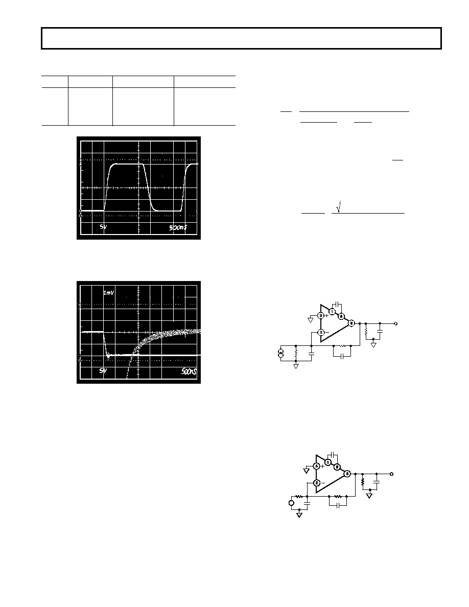
Table IV. Performance Summary for the 3 Op Amp
Instrumentation Amplifier Circuit
Gain
RG
Bandwidth
T Settle (0.01%)
1
NC
3.5 MHz
1.5
s
2
20 k
2.5 MHz
1.0
s
10
2.22 k
1 MHz
2
s
100
202
290 kHz
5
s
Figure 37. The Pulse Response of the 3 Op Amp
Instrumentation Amplifier. Gain = 1, l Horizontal Scale:
0.5
V/div., Vertical Scale: 5 V/div. (Gain= 10)
Figure 38. Settling Time of the 3 Op Amp Instrumentation
Amplifier. Horizontal Scale: 500 ns/div., Vertical Scale,
Pulse Input: 5 V/div., Output Settling: 1 mV/div.
Minimizing Settling Time in Real-World Applications
An amplifier with a “single pole” or “ideal” integrator open-loop
frequency response will achieve the minimum possible settling
time for any given unity-gain bandwidth. However, when this
“ideal” amplifier is used in a practical circuit, the actual settling
time is increased above the minimum value because of added
time constants which are introduced due to additional capacitance
on the amplifier’s summing junction. The following discussion
will explain how to minimize this increase in settling time by the
selection of the proper value for feedback capacitor, CL.
If an op amp is modeled as an ideal integrator with a unity gain
crossover frequency, fO, Equation 1 will accurately describe the
small signal behavior of the circuit of Figure 39. This circuit
models an op amp connected as an I-to-V converter.
Equation 1 would completely describe the output of the system
if not for the op amp’s finite slew rate and other nonlinear
effects. Even considering these effects, the fine scale settling to
<0.1% will be determined by the op amp’s small signal behav-
ior. Equation 1.
V
O
I
IN
=
– R
RC
L + CX
()
2
πF
O
s
2
+
G
N
2
πF
O
+ RC
L
s
+1
Where FO = the op amp’s unity gain crossover frequency
G
N = the “noise ” gain of the circuit
1
+
R
O
This Equation May Then Be Solved for CL:
Equation 2.
C
L =
2
G
N
R 2
πF
O
+
2 RC
X 2πFO + 1 GN
()
R 2
πF
O
In these equations, capacitance CX is the total capacitance appear-
ing at the inverting terminal of the op amp. When modeling an
I-to-V converter application, the Norton equivalent circuit of
Figure 39 can be used directly. Capacitance CX is the total capaci-
tance of the output of the current source plus the input capacitance
of the op amp, which includes any stray capacitance at the op
amp’s input.
AD744
CL
VOUT
RO
R
CCOMP (OPTIONAL)
CX
IO
RL
CLOAD
Figure 39. A Simplified Model of the AD744 Used as a
Current-to-Voltage Converter
When RO and IO are replaced with their Thevenin VIN and RIN
equivalents, the general purpose inverting amplifier model of
Figure 40 is created. Here capacitor CX represents the input
capacitance of the AD744 (5.5 pF) plus any stray capacitance
due to wiring and the type of IC package employed.
AD744
CL
VOUT
RIN
R
CCOMP (OPTIONAL)
CX
VIN
RL
CLOAD
Figure 40. A Simplified Model of the AD744 Used
as an Inverting Amplifier
相关PDF资料 |
PDF描述 |
|---|---|
| 172075-4 | CONN RCPT HSG 3POS .187 YELLOW |
| CL-130 | CURRENT LIMITER INRUSH |
| 75160-132-11LF | BERGSTIK |
| 02CO080.Z | FUSE 600V 80A HRCII-C BRIT DIM |
| RNCS0805BKE10R0 | RES 1/10W 10 OHM .1% 0805 |
相关代理商/技术参数 |
参数描述 |
|---|---|
| AD744BQ/+ | 制造商:Rochester Electronics LLC 功能描述:- Bulk |
| AD744CH | 制造商:Rochester Electronics LLC 功能描述:- Bulk |
| AD744CQ | 制造商:Rochester Electronics LLC 功能描述: 制造商:Analog Devices 功能描述: |
| AD744CQ/+ | 制造商:未知厂家 制造商全称:未知厂家 功能描述:Voltage-Feedback Operational Amplifier |
| AD744JCHIPS | 制造商:AD 制造商全称:Analog Devices 功能描述:Precision, 500 ns Settling BiFET Op Amp |
发布紧急采购,3分钟左右您将得到回复。