参数资料
| 型号: | AD7451BRMZ |
| 厂商: | Analog Devices Inc |
| 文件页数: | 24/25页 |
| 文件大小: | 0K |
| 描述: | IC ADC 12BIT DIFF 1MSPS 8MSOP |
| 标准包装: | 50 |
| 位数: | 12 |
| 采样率(每秒): | 1M |
| 数据接口: | DSP,MICROWIRE?,QSPI?,串行,SPI? |
| 转换器数目: | 1 |
| 功率耗散(最大): | 9.25mW |
| 电压电源: | 单电源 |
| 工作温度: | -40°C ~ 85°C |
| 安装类型: | 表面贴装 |
| 封装/外壳: | 8-TSSOP,8-MSOP(0.118",3.00mm 宽) |
| 供应商设备封装: | 8-MSOP |
| 包装: | 管件 |
| 输入数目和类型: | 1 个伪差分,单极 |
AD7441/AD7451
Rev. D | Page 7 of 24
TIMING SPECIFICATIONS1
VDD = 2.7 V to 5.25 V; fSCLK = 18 MHz; fS = 1 MSPS; VREF = 2.5 V; TA = TMIN to TMAX, unless otherwise noted.
Table 3.
Parameter
Limit at TMIN, TMAX
Unit
Description
10
kHz min
18
MHz max
tCONVERT
16 × tSCLK
tSCLK = 1/fSCLK
888
ns max
tQUIET
60
ns min
Minimum quiet time between end of a serial read and next falling edge of CS
t1
10
ns min
Minimum CS pulse width
t2
10
ns min
CS falling edge to SCLK falling edge setup time
20
ns max
Delay from CS falling edge until SDATA three-state disabled
t4
40
ns max
Data access time after SCLK falling edge
t5
0.4 tSCLK
ns min
SCLK high pulse width
t6
0.4 tSCLK
ns min
SCLK low pulse width
t7
10
ns min
SCLK edge to data valid hold time
10
ns min
SCLK falling edge to SDATA, three-state enabled
35
ns max
SCLK falling edge to SDATA, three-state enabled
tPOWER-UP5
1
μs max
Power-up time from full power-down
1 Guaranteed by characterization. All input signals are specified with tRISE = tFALL = 5 ns (10% to 90% of VDD) and timed from a voltage level of 1.6 V. See Figure 2, Figure 3,
and the Serial Interface section.
2 Mark/space ratio for the SCLK input is 40/60 to 60/40.
3 Measured with the load circuit of Figure 4 and defined as the time required for the output to cross 0.8 V or 2.4 V with VDD = 5 V and the time required for an output to
cross 0.4 V or 2.0 V for VDD = 3 V.
4 t8 is derived from the measured time taken by the data outputs to change 0.5 V when loaded with the circuit of Figure 4. The measured number is then extrapolated
back to remove the effects of charging or discharging the 25 pF capacitor. This means that the time (t8) quoted in the timing characteristics is the true bus relinquish
time of the part and is independent of the bus loading.
5 See the Power-Up Time section.
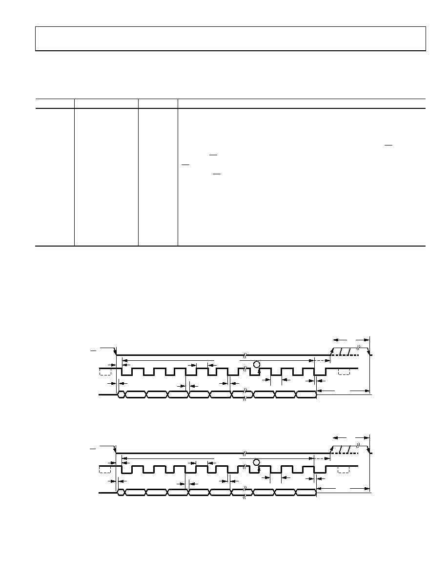
TIMING DIAGRAMS
t3
t2
t4
t7
t8
t6
t1
t5
tQUIET
tCONVERT
CS
SCLK
SDATA
4 LEADING ZEROS
THREE-STATE
12
3
4
5
13
14
15
16
0
DB11
DB10
DB2
DB1
DB0
B
03
15
3-
0
02
Figure 2. AD7451 Serial Interface Timing Diagram
t3
t2
t4
t7
t8
t6
t1
t5
tQUIET
tCONVERT
CS
SCLK
SDATA
4 LEADING ZEROS
2 TRAILING ZEROS THREE-STATE
12
3
4
5
13
14
15
16
0
DB9
DB8
DB0
0
B
03
15
3-
0
03
Figure 3. AD7441 Serial Interface Timing Diagram
相关PDF资料 |
PDF描述 |
|---|---|
| AD7452BRT-R2 | IC ADC 12BIT 555KSPS SOT23-8 |
| AD7453BRTZ-REEL7 | IC ADC 12BIT W/DIFF INP SOT23-8 |
| AD7457BRTZ-REEL7 | IC ADC 12BIT PSEUDO-DIFF SOT23-8 |
| AD7467BRTZ-REEL | IC ADC 10BIT 1.6V MCRPWR SOT23-6 |
| AD7472ARU-REEL | IC ADC 12BIT PARALLEL 24-TSSOP |
相关代理商/技术参数 |
参数描述 |
|---|---|
| AD7451BRMZ | 制造商:Analog Devices 功能描述:12BIT SAR ADC DIFF I/P SMD 7451 |
| AD7451BRT | 制造商:AD 制造商全称:Analog Devices 功能描述:Pseudo Differential, 1MSPS, 12- & 10-Bit ADCs in 8-lead SOT-23 |
| AD7451BRT-R2 | 功能描述:IC ADC 12BIT W/DIFF INP SOT-23-8 RoHS:否 类别:集成电路 (IC) >> 数据采集 - 模数转换器 系列:- 产品培训模块:Lead (SnPb) Finish for COTS Obsolescence Mitigation Program 标准包装:2,500 系列:- 位数:12 采样率(每秒):3M 数据接口:- 转换器数目:- 功率耗散(最大):- 电压电源:- 工作温度:- 安装类型:表面贴装 封装/外壳:SOT-23-6 供应商设备封装:SOT-23-6 包装:带卷 (TR) 输入数目和类型:- |
| AD7451BRT-REEL7 | 制造商:Analog Devices 功能描述: |
| AD7452 | 制造商:AD 制造商全称:Analog Devices 功能描述:Differential Input, 555 kSPS 12-Bit ADC in an 8-Lead SOT-23 |
发布紧急采购,3分钟左右您将得到回复。