- 您现在的位置:买卖IC网 > PDF目录1981 > AD7453BRTZ-REEL7 (Analog Devices Inc)IC ADC 12BIT W/DIFF INP SOT23-8 PDF资料下载
参数资料
| 型号: | AD7453BRTZ-REEL7 |
| 厂商: | Analog Devices Inc |
| 文件页数: | 4/21页 |
| 文件大小: | 0K |
| 描述: | IC ADC 12BIT W/DIFF INP SOT23-8 |
| 设计资源: | Measuring -48 V High-Side Current Using AD629, AD8603, AD780, and AD7453 (CN0100) |
| 标准包装: | 3,000 |
| 位数: | 12 |
| 采样率(每秒): | 555k |
| 数据接口: | DSP,MICROWIRE?,QSPI?,串行,SPI? |
| 转换器数目: | 1 |
| 功率耗散(最大): | 7.25mW |
| 电压电源: | 单电源 |
| 工作温度: | -40°C ~ 85°C |
| 安装类型: | 表面贴装 |
| 封装/外壳: | SOT-23-8 |
| 供应商设备封装: | SOT-23-8 |
| 包装: | 带卷 (TR) |
| 输入数目和类型: | 1 个伪差分,双极 |
AD7453
Rev. B | Page 11 of 20
CIRCUIT INFORMATION
The AD7453 is a 12-bit, low power, single-supply, successive
approximation analog-to-digital converter (ADC) with a
pseudo differential analog input. It operates with a single 2.7 V
to 5.25 V power supply and is capable of throughput rates up to
555 kSPS when supplied with a 10 MHz SCLK. It requires an
external reference to be applied to the VREF pin.
The AD7453 has an on-chip differential track-and-hold
amplifier, a successive approximation (SAR) ADC, and a serial
interface, housed in an 8-lead SOT-23 package. The serial clock
input accesses data from the part and provides the clock source
for the successive approximation ADC. The AD7453 features a
power-down option for reduced power consumption between
conversions. The power-down feature is implemented across the
standard serial interface, as described in the Modes of
Operation section.
CONVERTER OPERATION
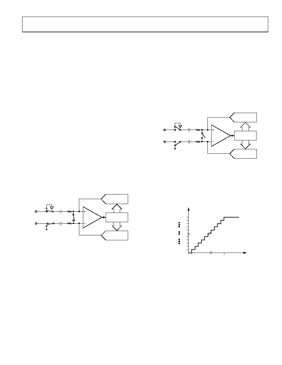
The AD7453 is a successive approximation ADC based around
schematics of the ADC in the acquisition and conversion phase,
respectively. The ADC is comprised of control logic, an SAR,
and two capacitive DACs. In Figure 14 (acquisition phase), SW3
is closed and SW1 and SW2 are in Position A, the comparator is
held in a balanced condition, and the sampling capacitor arrays
acquire the differential signal on the input.
VIN+
VIN–
A
B
SW1
SW3
COMPARATOR
CONTROL
LOGIC
CAPACITIVE
DAC
CAPACITIVE
DAC
CS
VREF
SW2
B
A
03155-A
-014
Figure 14. ADC Acquisition Phase
When the ADC starts a conversion (Figure 15), SW3 opens and
SW1 and SW2 move to Position B, causing the comparator to
become unbalanced. Both inputs are disconnected once the
conversion begins. The control logic and charge redistribution
DACs are used to add and subtract fixed amounts of charge
from the sampling capacitor arrays to bring the comparator
back into a balanced condition. When the comparator is rebal-
anced, the conversion is complete. The control logic generates
the ADC’s output code. The output impedances of the sources
driving the VIN+ and VIN– pins must be matched; otherwise the
two inputs have different settling times, resulting in errors.
VIN+
VIN–
A
B
SW1
SW3
CONTROL
LOGIC
CAPACITIVE
DAC
CAPACITIVE
DAC
CS
VREF
SW2
B
A
03155-A
-015
COMPARATOR
Figure 15. ADC Conversion Phase
ADC TRANSFER FUNCTION
The output coding for the AD7453 is straight (natural) binary.
The designed code transitions occur at successive LSB values
(i.e., 1 LSB, 2 LSB, and so on). The LSB size is VREF/4096. The
ideal transfer characteristic of the AD7453 is shown in
000...00
0V
ADC
CO
DE
ANALOG INPUT
111...11
000...01
111...00
011...11
1LSB
VREF – 1LSB
1LSB = VREF/4096
111...10
000...10
03155-A
-016
Figure 16. Ideal Transfer Characteristic
相关PDF资料 |
PDF描述 |
|---|---|
| AD7457BRTZ-REEL7 | IC ADC 12BIT PSEUDO-DIFF SOT23-8 |
| AD7467BRTZ-REEL | IC ADC 10BIT 1.6V MCRPWR SOT23-6 |
| AD7472ARU-REEL | IC ADC 12BIT PARALLEL 24-TSSOP |
| AD7476ABRM | IC ADC 12BIT 2.35V 1MSPS 8-MSOP |
| AD7478ARTZ-REEL | IC ADC 8BIT 1MSPS SOT23-6 |
相关代理商/技术参数 |
参数描述 |
|---|---|
| AD7457 | 制造商:AD 制造商全称:Analog Devices 功能描述:Low Power, Pseudo Differential, 100 kSPS 12-Bit ADC in an 8-Lead SOT-23 |
| AD7457_05 | 制造商:AD 制造商全称:Analog Devices 功能描述:Low Power, Pseudo Differential, 100 kSPS |
| AD7457BRT | 制造商:Analog Devices 功能描述: |
| AD7457BRT-R2 | 制造商:Analog Devices 功能描述:ADC Single SAR 100ksps 12-bit Serial 8-Pin SOT-23 T/R 制造商:Rochester Electronics LLC 功能描述:12-BIT P/DIFF I/PUT, 100KSPS ADC I.C. - Bulk |
| AD7457BRT-REEL | 制造商:Analog Devices 功能描述:ADC SGL SAR 100KSPS 12-BIT SERL 8PIN SOT-23 - Tape and Reel |
发布紧急采购,3分钟左右您将得到回复。