- 您现在的位置:买卖IC网 > PDF目录3432 > AD745JRZ-16-REEL7 (Analog Devices Inc)IC OPAMP BIFET 20MHZ ULN 16SOIC PDF资料下载
参数资料
| 型号: | AD745JRZ-16-REEL7 |
| 厂商: | Analog Devices Inc |
| 文件页数: | 3/12页 |
| 文件大小: | 0K |
| 描述: | IC OPAMP BIFET 20MHZ ULN 16SOIC |
| 标准包装: | 400 |
| 放大器类型: | J-FET |
| 电路数: | 1 |
| 转换速率: | 12.5 V/µs |
| 增益带宽积: | 20MHz |
| -3db带宽: | 20MHz |
| 电流 - 输入偏压: | 150pA |
| 电压 - 输入偏移: | 250µV |
| 电流 - 电源: | 8mA |
| 电流 - 输出 / 通道: | 40mA |
| 电压 - 电源,单路/双路(±): | 9.6 V ~ 36 V,±4.8 V ~ 18 V |
| 工作温度: | 0°C ~ 70°C |
| 安装类型: | 表面贴装 |
| 封装/外壳: | 16-SOIC(0.295",7.50mm 宽) |
| 供应商设备封装: | 16-SOIC W |
| 包装: | 带卷 (TR) |
REV. D
AD745
–11–
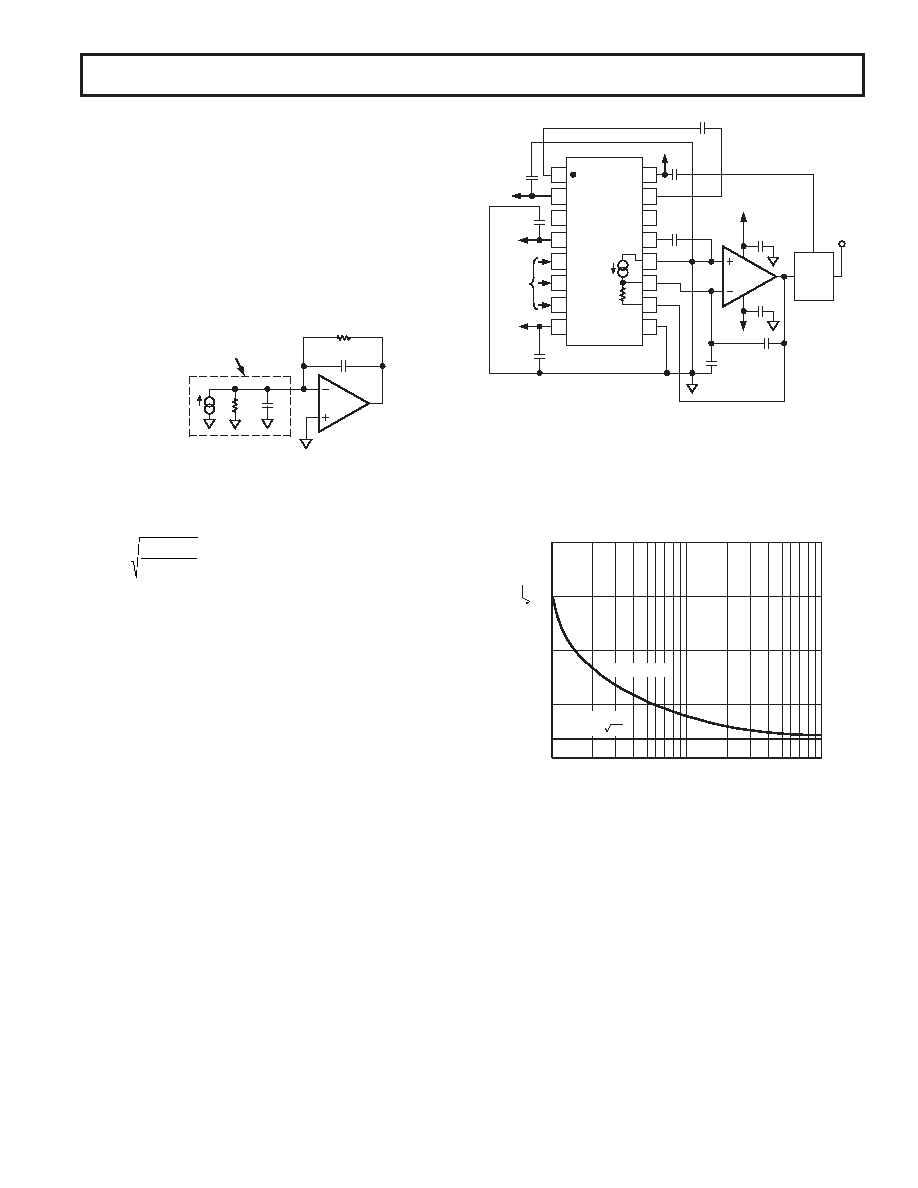
DESIGN CONSIDERATIONS FOR I-TO-V CONVERTERS
There are some simple rules of thumb when designing an I-V
converter where there is significant source capacitance (as with
a photodiode) and bandwidth needs to be optimized. Consider
the circuit of Figure 18. The high frequency noise gain
(1 + CS/CL) is usually greater than five, so the AD745, with its
higher slew rate and bandwidth is ideally suited to this applica-
tion.
Here both the low current and low voltage noise of the AD745 can
be taken advantage of, since it is desirable in some instances to
have a large RF (which increases sensitivity to input current noise)
and, at the same time, operate the amplifier at high noise gain.
AD745
IS
RB
CS
CL
RF
INPUT SOURCE: PHOTO DIODE,
ACCELEROMETER, ECT.
Figure 18. A Model for an l-to-V Converter
In this circuit, the RF CS time constant limits the practical band-
width over which flat response can be obtained, in fact:
f
B ≈
f
C
2
π R
FCS
where:
fB = signal bandwidth
fC = gain bandwidth product of the amplifier
With CL
≈ 1/(2 πRF CS) the net response can be adjusted to a
provide a two pole system with optimal flatness that has a corner
frequency of fB. Capacitor CL adjusts the damping of the circuit’s
response. Note that bandwidth and sensitivity are directly traded
off against each other via the selection of RF. For example, a
photodiode with CS = 300 pF and RF = 100 k
will have a maxi-
mum bandwidth of 360 kHz when capacitor CL
≈ 4.5 pF.
Conversely, if only a 100 kHz bandwidth were required, then
the maximum value of RF would be 360 k
and that of capaci-
tor CL still
≈ 4.5 pF.
In either case, the AD745 provides impedance transformation,
the effective transresistance, i.e., the I/V conversion gain, may
be augmented with further gain. A wideband low noise amplifier
such as the AD829 is recommended in this application.
This principle can also be used to apply the AD745 in a high
performance audio application. Figure 19 shows that an I-V
converter of a high performance DAC, here the AD1862, can
be designed to take advantage of the low voltage noise of the
AD745 (2.9 nV/ Hz) as well as the high slew rate and band-
width provided by decompensation. This circuit, with component
values shown, has a 12 dB/octave rolloff at 728 kHz, with a
passband ripple of less than 0.001 dB and a phase deviation of
less than 2 degrees @ 20 kHz.
0.1 F
AD745
0.1 F
+12V
–12V
100pF
2000pF
10 F
+
DIGITAL
COMMON
0.01 F
–12V
AD1862
20-BIT D/A
CONVERTER
3k
TOP VIEW
3 POLE
LOW
PASS
FILTER
OUTPUT
0.01 F
ANALOG
COMMON
+12V
DIGITAL
INPUTS
+12V
0.01 F
–12V
0.01 F
1 F
+
16
15
14
13
12
11
10
9
1
2
3
4
5
6
7
8
Figure 19. A High Performance Audio DAC Circuit
An important feature of this circuit is that high frequency en-
ergy, such as clock feedthrough, is shunted to common via a
high quality capacitor and not the output stage of the amplifier,
greatly reducing the error signal at the input of the amplifier and
subsequent opportunities for intermodulation distortions.
INPUT CAPACITANCE – pF
40
30
0
10
1k
100
R
T
INOISE
V
O
L
T
A
GE
–
nV/
Hz
20
10
BALANCED
2.9nV/ Hz
UNBALANCED
Figure 20. RTI Noise Voltage vs. Input Capacitance
BALANCING SOURCE IMPEDANCES
As mentioned previously, it is good practice to balance the
source impedances (both resistive and reactive) as seen by the
inputs of the AD745. Balancing the resistive components will
optimize dc performance over temperature because balancing
will mitigate the effects of any bias current errors. Balancing
input capacitance will minimize ac response errors due to the
amplifier’s input capacitance and, as shown in Figure 20, noise
performance will be optimized. Figure 21 shows the required
external components for noninverting (A) and inverting (B)
configurations.
相关PDF资料 |
PDF描述 |
|---|---|
| 2036-42-C2LF | GAS DISCHARGE TUBE |
| 77313-818-42LF | CONN HEADER .100 DUAL STR 42POS |
| 78548-152HLF | BERGSTIK II DR STRAIGHT RET |
| 65863-025LF | 65863-25-QKE HDR LF |
| 65863-025 | QKE HDR |
相关代理商/技术参数 |
参数描述 |
|---|---|
| AD745KN | 制造商:Rochester Electronics LLC 功能描述:- Bulk 制造商:Analog Devices 功能描述: |
| AD745KR-16 | 功能描述:IC OPAMP BIFET 20MHZ ULN 16SOIC RoHS:否 类别:集成电路 (IC) >> Linear - Amplifiers - Instrumentation 系列:- 标准包装:50 系列:- 放大器类型:J-FET 电路数:2 输出类型:- 转换速率:3.5 V/µs 增益带宽积:1MHz -3db带宽:- 电流 - 输入偏压:30pA 电压 - 输入偏移:2000µV 电流 - 电源:200µA 电流 - 输出 / 通道:- 电压 - 电源,单路/双路(±):7 V ~ 36 V,±3.5 V ~ 18 V 工作温度:0°C ~ 70°C 安装类型:通孔 封装/外壳:8-DIP(0.300",7.62mm) 供应商设备封装:8-PDIP 包装:管件 |
| AD745KR-16-REEL | 功能描述:IC OPAMP BIFET 20MHZ ULN 16SOIC RoHS:否 类别:集成电路 (IC) >> Linear - Amplifiers - Instrumentation 系列:- 标准包装:2,500 系列:Excalibur™ 放大器类型:J-FET 电路数:1 输出类型:- 转换速率:45 V/µs 增益带宽积:10MHz -3db带宽:- 电流 - 输入偏压:20pA 电压 - 输入偏移:490µV 电流 - 电源:1.7mA 电流 - 输出 / 通道:48mA 电压 - 电源,单路/双路(±):4.5 V ~ 38 V,±2.25 V ~ 19 V 工作温度:-40°C ~ 85°C 安装类型:表面贴装 封装/外壳:8-SOIC(0.154",3.90mm 宽) 供应商设备封装:8-SOIC 包装:带卷 (TR) |
| AD745KR-16-REEL7 | 功能描述:IC OPAMP BIFET 20MHZ ULN 16SOIC RoHS:否 类别:集成电路 (IC) >> Linear - Amplifiers - Instrumentation 系列:- 标准包装:2,500 系列:Excalibur™ 放大器类型:J-FET 电路数:1 输出类型:- 转换速率:45 V/µs 增益带宽积:10MHz -3db带宽:- 电流 - 输入偏压:20pA 电压 - 输入偏移:490µV 电流 - 电源:1.7mA 电流 - 输出 / 通道:48mA 电压 - 电源,单路/双路(±):4.5 V ~ 38 V,±2.25 V ~ 19 V 工作温度:-40°C ~ 85°C 安装类型:表面贴装 封装/外壳:8-SOIC(0.154",3.90mm 宽) 供应商设备封装:8-SOIC 包装:带卷 (TR) |
| AD745KRZ-16 | 功能描述:IC OPAMP BIFET 20MHZ ULN 16SOIC RoHS:是 类别:集成电路 (IC) >> Linear - Amplifiers - Instrumentation 系列:- 标准包装:2,500 系列:- 放大器类型:通用 电路数:4 输出类型:- 转换速率:0.6 V/µs 增益带宽积:1MHz -3db带宽:- 电流 - 输入偏压:45nA 电压 - 输入偏移:2000µV 电流 - 电源:1.4mA 电流 - 输出 / 通道:40mA 电压 - 电源,单路/双路(±):3 V ~ 32 V,±1.5 V ~ 16 V 工作温度:0°C ~ 70°C 安装类型:表面贴装 封装/外壳:14-TSSOP(0.173",4.40mm 宽) 供应商设备封装:14-TSSOP 包装:带卷 (TR) 其它名称:LM324ADTBR2G-NDLM324ADTBR2GOSTR |
发布紧急采购,3分钟左右您将得到回复。