参数资料
| 型号: | AD7476ABRM |
| 厂商: | Analog Devices Inc |
| 文件页数: | 29/29页 |
| 文件大小: | 0K |
| 描述: | IC ADC 12BIT 2.35V 1MSPS 8-MSOP |
| 设计资源: | Output Channel Monitoring Using AD5380 (CN0008) AD5382 Channel Monitor Function (CN0012) AD5381 Channel Monitor Function (CN0013) AD5383 Channel Monitor Function (CN0015) AD5390/91/92 Channel Monitor Function (CN0030) Power off protected data acquisition signal chain using ADG4612 , AD711, and AD7476 (CN0165) |
| 标准包装: | 50 |
| 位数: | 12 |
| 采样率(每秒): | 1M |
| 数据接口: | DSP,MICROWIRE?,QSPI?,串行,SPI? |
| 转换器数目: | 1 |
| 功率耗散(最大): | 17.5mW |
| 电压电源: | 单电源 |
| 工作温度: | -40°C ~ 85°C |
| 安装类型: | 表面贴装 |
| 封装/外壳: | 8-TSSOP,8-MSOP(0.118",3.00mm 宽) |
| 供应商设备封装: | 8-MSOP |
| 包装: | 管件 |
| 输入数目和类型: | 1 个单端,单极 |
| 配用: | EVAL-AD7476ACBZ-ND - BOARD EVALUATION FOR AD7476A |
第1页第2页第3页第4页第5页第6页第7页第8页第9页第10页第11页第12页第13页第14页第15页第16页第17页第18页第19页第20页第21页第22页第23页第24页第25页第26页第27页第28页当前第29页
AD7476A/AD7477A/AD7478A
Rev. F | Page 8 of 28
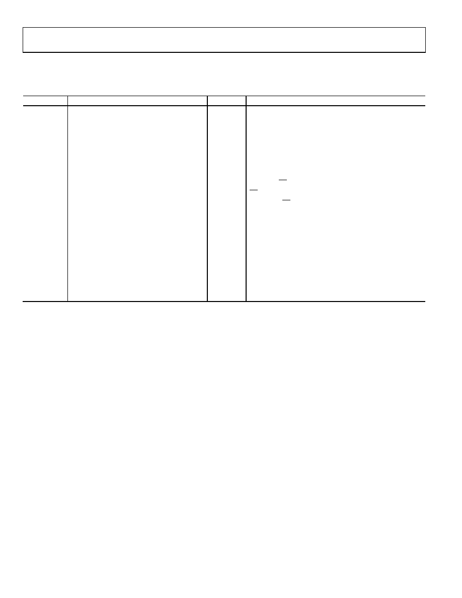
TIMING SPECIFICATIONS
Table 4.
Parameter
Limit at TMIN, TMAX
Unit
Description
fSCLK2
10
kHz min3
A, B grades
20
kHz min3
Y grade
20
MHz max
tCONVERT
16 × tSCLK
AD7476A
14 × tSCLK
AD7477A
12 × tSCLK
AD7478A
tQUIET
50
ns min
Minimum quiet time required between bus relinquish
and start of next conversion
t1
10
ns min
Minimum CS pulse width
t2
10
ns min
CS to SCLK setup time
t34
22
ns max
Delay from CS until SDATA three-state disabled
t44
40
ns max
Data access time after SCLK falling edge
t5
0.4 tSCLK
ns min
SCLK low pulse width
t6
0.4 tSCLK
ns min
SCLK high pulse width
t75
SCLK to data valid hold time
10
ns min
VDD ≤ 3.3 V
9.5
ns min
3.3 V < VDD ≤ 3.6 V
7
ns min
VDD > 3.6 V
t86
36
ns max
SCLK falling edge to SDATA high impedance
t7 values also apply to t8 minimum values
ns min
SCLK falling edge to SDATA high impedance
tPOWER-UP7
1
μs max
Power-up time from full power-down
1
Guaranteed by characterization. All input signals are specified with tr = tf = 5 ns (10% to 90% of VDD) and timed from a voltage level of 1.6 V.
2
Mark/space ratio for the SCLK input is 40/60 to 60/40.
3
Minimum fSCLK at which specifications are guaranteed.
4
Measured with the load circuit shown in Figure 2, and defined as the time required for the output to cross 0.8 V or 1.8 V when VDD = 2.35 V, and
0.8 V or 2.0 V for VDD > 2.35 V.
5
Measured with a 50 pF load capacitor.
6
t8 is derived from the measured time taken by the data outputs to change 0.5 V when loaded with the circuit shown in Figure 2. The measured number is then
extrapolated back to remove the effects of charging or discharging the 50 pF capacitor. Therefore, the time, t8, quoted in the timing characteristics is the true bus
relinquish time of the part and is independent of the bus loading.
7
See the Power-Up Time section.
相关PDF资料 |
PDF描述 |
|---|---|
| AD7478ARTZ-REEL | IC ADC 8BIT 1MSPS SOT23-6 |
| AD7482ASTZ | IC ADC 12BIT SAR 3MSPS 48LQFP |
| AD7484BSTZ | IC ADC 14BIT SAR 3MSPS 48-LQFP |
| AD7485BSTZ | IC ADC 14BIT SAR 1MSPS 48-LQFP |
| AD7490BRU-REEL | IC ADC 12BIT 16CH 28-TSSOP T/R |
相关代理商/技术参数 |
参数描述 |
|---|---|
| AD7476ABRM-REEL | 功能描述:IC ADC 12BIT 1MSPS 8-MSOP T/R RoHS:否 类别:集成电路 (IC) >> 数据采集 - 模数转换器 系列:- 标准包装:1,000 系列:- 位数:16 采样率(每秒):45k 数据接口:串行 转换器数目:2 功率耗散(最大):315mW 电压电源:模拟和数字 工作温度:0°C ~ 70°C 安装类型:表面贴装 封装/外壳:28-SOIC(0.295",7.50mm 宽) 供应商设备封装:28-SOIC W 包装:带卷 (TR) 输入数目和类型:2 个单端,单极 |
| AD7476ABRM-REEL7 | 功能描述:IC ADC 12BIT 1MSPS 8-MSOP T/R RoHS:否 类别:集成电路 (IC) >> 数据采集 - 模数转换器 系列:- 标准包装:1,000 系列:- 位数:16 采样率(每秒):45k 数据接口:串行 转换器数目:2 功率耗散(最大):315mW 电压电源:模拟和数字 工作温度:0°C ~ 70°C 安装类型:表面贴装 封装/外壳:28-SOIC(0.295",7.50mm 宽) 供应商设备封装:28-SOIC W 包装:带卷 (TR) 输入数目和类型:2 个单端,单极 |
| AD7476ABRMZ | 功能描述:IC ADC 12BIT 1MSPS 8-MSOP RoHS:是 类别:集成电路 (IC) >> 数据采集 - 模数转换器 系列:- 其它有关文件:TSA1204 View All Specifications 标准包装:1 系列:- 位数:12 采样率(每秒):20M 数据接口:并联 转换器数目:2 功率耗散(最大):155mW 电压电源:模拟和数字 工作温度:-40°C ~ 85°C 安装类型:表面贴装 封装/外壳:48-TQFP 供应商设备封装:48-TQFP(7x7) 包装:Digi-Reel® 输入数目和类型:4 个单端,单极;2 个差分,单极 产品目录页面:1156 (CN2011-ZH PDF) 其它名称:497-5435-6 |
| AD7476ABRMZ | 制造商:Analog Devices 功能描述:IC 12BIT ADC SMD 7476 MSOP8 |
| AD7476ABRMZ-REEL | 功能描述:IC ADC 12BIT 1MSPS 8-MSOP RoHS:是 类别:集成电路 (IC) >> 数据采集 - 模数转换器 系列:- 标准包装:1,000 系列:- 位数:16 采样率(每秒):45k 数据接口:串行 转换器数目:2 功率耗散(最大):315mW 电压电源:模拟和数字 工作温度:0°C ~ 70°C 安装类型:表面贴装 封装/外壳:28-SOIC(0.295",7.50mm 宽) 供应商设备封装:28-SOIC W 包装:带卷 (TR) 输入数目和类型:2 个单端,单极 |
发布紧急采购,3分钟左右您将得到回复。