- 您现在的位置:买卖IC网 > PDF目录10688 > AD7476ARTZ-500RL7 (Analog Devices Inc)IC ADC 12BIT 1MSPS SOT-23-6 PDF资料下载
参数资料
| 型号: | AD7476ARTZ-500RL7 |
| 厂商: | Analog Devices Inc |
| 文件页数: | 8/25页 |
| 文件大小: | 0K |
| 描述: | IC ADC 12BIT 1MSPS SOT-23-6 |
| 设计资源: | Output Channel Monitoring Using AD5380 (CN0008) AD5382 Channel Monitor Function (CN0012) AD5381 Channel Monitor Function (CN0013) AD5383 Channel Monitor Function (CN0015) AD5390/91/92 Channel Monitor Function (CN0030) Power off protected data acquisition signal chain using ADG4612 , AD711, and AD7476 (CN0165) |
| 标准包装: | 1 |
| 位数: | 12 |
| 采样率(每秒): | 1M |
| 数据接口: | DSP,MICROWIRE?,QSPI?,串行,SPI? |
| 转换器数目: | 1 |
| 功率耗散(最大): | 17.5mW |
| 电压电源: | 单电源 |
| 工作温度: | -40°C ~ 85°C |
| 安装类型: | 表面贴装 |
| 封装/外壳: | SOT-23-6 |
| 供应商设备封装: | SOT-23-6 |
| 包装: | 标准包装 |
| 输入数目和类型: | 1 个单端,单极 |
| 产品目录页面: | 777 (CN2011-ZH PDF) |
| 配用: | EVAL-AD7476ACBZ-ND - BOARD EVALUATION FOR AD7476A |
| 其它名称: | AD7476ARTZ-500RL7DKR |
AD7476/AD7477/AD7478
Rev. F | Page 15 of 24
0
–10
–20
–30
–40
–50
–60
–70
–80
–90
–100
1
10k
1k
100
10
01
02
4-
01
6
T
HD
(
d
B)
SOURCE IMPEDANCE (
)
fIN = 200kHz
fIN = 300kHz
fIN = 100kHz
fIN = 10kHz
VDD = 2.7V
fS = 605kSPS
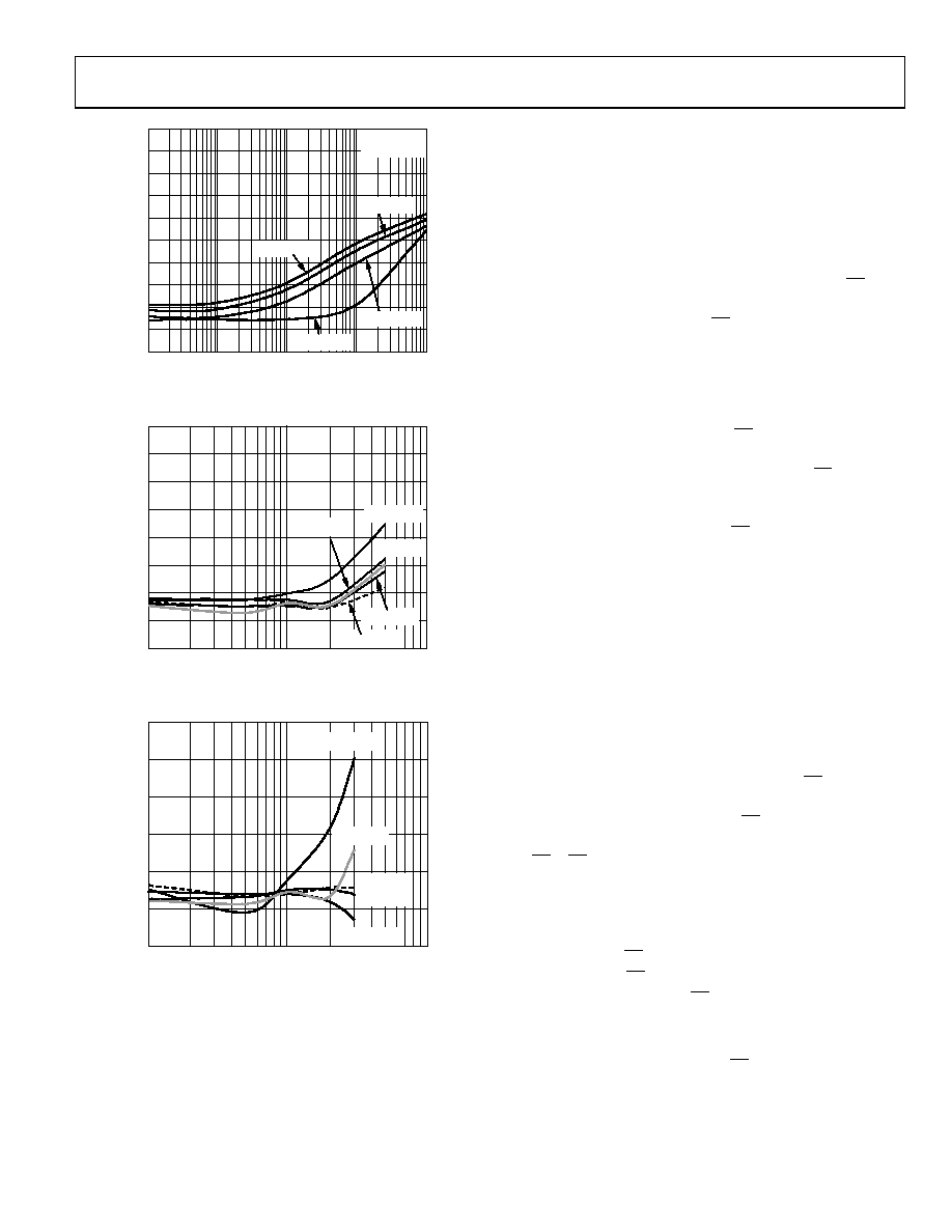
Figure 16. THD vs. Source Impedance for Various Analog Input Frequencies
VDD = 2.35V
VDD = 5.25V
VDD = 2.7V
VDD = 4.75V
VDD = 3.6V
–50
–90
–85
–80
–75
–70
–65
–60
–55
10k
1M
100k
01
02
4-
01
7
T
HD
(
d
B)
INPUT FREQUENCY (Hz)
Figure 17. THD vs. Analog Input Frequency, fs = 993 kSPS
VDD = 2.35V
VDD = 3.6V
–72
–74
–76
–78
–80
–82
–84
10k
1M
100k
01
02
4-
01
8
T
HD
(
d
B)
INPUT FREQUENCY (Hz)
VDD = 4.75V
VDD = 5.25V
VDD = 2.7V
Figure 18. THD vs. Analog Input Frequency, fs = 605 kSPS
Digital Input
The digital input applied to the AD7476/AD7477/AD7478 is
not limited by the maximum ratings that limit the analog input.
Instead, the digital input applied can go to 7 V and is not
restricted by the VDD + 0.3 V limit as on the analog input. For
example, if the AD7476/AD7477/AD7478 are operated with a
VDD of 3 V, then 5 V logic levels can be used on the digital input.
However, note that the data output on SDATA still has 3 V logic
levels when VDD = 3 V. Another advantage of SCLK and CS not
being restricted by the VDD + 0.3 V limit is that power supply
sequencing issues are avoided. If CS or SCLK is applied before
VDD, there is no risk of latch-up as there is on the analog input
when a signal greater than 0.3 V is applied prior to VDD.
MODES OF OPERATION
Select the mode of operation of the AD7476/AD7477/AD7478
by controlling the (logic) state of the CS signal during a
conversion. The two possible modes of operation are normal
mode and power-down mode. The point at which CS is pulled
high after the conversion has been initiated determines whether
or not the AD7476/AD7477/AD7478 enters power-down mode.
Similarly, if already in power-down, CS can control whether the
device returns to normal operation or remains in power-down.
These modes of operation are designed to provide flexible
power management options. These options can be chosen to
optimize the power dissipation/throughput rate ratio for
different application requirements.
Normal Mode
This mode is intended for fastest throughput rate performance.
Users do not have to worry about power-up times with the
AD7476/AD7477/AD7478 remaining fully powered at all times.
Figure 19 shows the general diagram of the AD7476/AD7477/
AD7478 in normal mode.
The conversion is initiated on the falling edge of CS as de-
scribed in the
section. To ensure the part
remains fully powered up at all times,
CS must remain low until
at least 10 SCLK falling edges have elapsed after the falling edge
of CS. If CS is brought high any time after the tenth SCLK
falling edge, but before the sixteenth SCLK falling edge, the part
remains powered up, but the conversion terminates and SDATA
goes back into three-state. Sixteen serial clock cycles are
required to complete the conversion and access the complete
conversion result. CS may idle high until the next conversion or
may idle low until CS returns high sometime prior to the next
conversion (effectively idling CS low).
Once a data transfer is complete, (SDATA has returned to three-
state), another conversion can be initiated after the quiet time,
tQUIET, has elapsed by again bringing CS low.
相关PDF资料 |
PDF描述 |
|---|---|
| LTC1445CS#TR | IC COMP QUAD LP 1.221VREF 16SOIC |
| LTC1444CS#TRPBF | IC COMP W/REF LOWPWR QUAD 16SOIC |
| VE-230-MY-B1 | CONVERTER MOD DC/DC 5V 50W |
| VI-2TT-IX-B1 | CONVERTER MOD DC/DC 6.5V 75W |
| AD8611ARMZ-REEL | IC COMP SGL 4NS ULTRFAST 8MSOP |
相关代理商/技术参数 |
参数描述 |
|---|---|
| AD7476ARTZ-500RL7 | 制造商:Analog Devices 功能描述:IC 12BIT ADC 1MSPS SOT23-6 制造商:Analog Devices 功能描述:IC, 12BIT ADC, 1MSPS, SOT23-6 |
| AD7476ARTZ-500RL73 | 制造商:AD 制造商全称:Analog Devices 功能描述:1 MSPS, 12-/10-/8-Bit ADCs in 6-Lead SOT-23 |
| AD7476ARTZ-REEL | 功能描述:IC ADC 12BIT 1MSPS SOT23-6 RoHS:是 类别:集成电路 (IC) >> 数据采集 - 模数转换器 系列:- 标准包装:1,000 系列:- 位数:16 采样率(每秒):45k 数据接口:串行 转换器数目:2 功率耗散(最大):315mW 电压电源:模拟和数字 工作温度:0°C ~ 70°C 安装类型:表面贴装 封装/外壳:28-SOIC(0.295",7.50mm 宽) 供应商设备封装:28-SOIC W 包装:带卷 (TR) 输入数目和类型:2 个单端,单极 |
| AD7476ARTZ-REEL3 | 制造商:AD 制造商全称:Analog Devices 功能描述:1 MSPS, 12-/10-/8-Bit ADCs in 6-Lead SOT-23 |
| AD7476ARTZ-REEL7 | 功能描述:IC ADC 12BIT 1MSPS LP SOT23-6 RoHS:是 类别:集成电路 (IC) >> 数据采集 - 模数转换器 系列:- 标准包装:1,000 系列:- 位数:16 采样率(每秒):45k 数据接口:串行 转换器数目:2 功率耗散(最大):315mW 电压电源:模拟和数字 工作温度:0°C ~ 70°C 安装类型:表面贴装 封装/外壳:28-SOIC(0.295",7.50mm 宽) 供应商设备封装:28-SOIC W 包装:带卷 (TR) 输入数目和类型:2 个单端,单极 |
发布紧急采购,3分钟左右您将得到回复。