- 您现在的位置:买卖IC网 > PDF目录373901 > AD7476BRT (ANALOG DEVICES INC) +3.3V, 2.125Gbps/1.0625Gbps Fibre-Channel Port Bypass ICs PDF资料下载
参数资料
| 型号: | AD7476BRT |
| 厂商: | ANALOG DEVICES INC |
| 元件分类: | ADC |
| 英文描述: | +3.3V, 2.125Gbps/1.0625Gbps Fibre-Channel Port Bypass ICs |
| 中文描述: | 1-CH 12-BIT SUCCESSIVE APPROXIMATION ADC, SERIAL ACCESS, PDSO6 |
| 封装: | PLASTIC, MO-178AB, SOT-23, 6 PIN |
| 文件页数: | 10/20页 |
| 文件大小: | 360K |
| 代理商: | AD7476BRT |
REV. D
–10–
AD7476/AD7477/AD7478
CIRCUIT INFORMATION
The AD7476/AD7477/AD7478 are, respectively, 12-bit, 10-bit,
and 8-bit, fast, micropower, single-supply ADCs. The parts can be
operated from a 2.35 V to 5.25 V supply. When operated from
either a 5 V supply or a 3 V supply, the AD7476/AD7477/AD7478
are capable of throughput rates of 1 MSPS when provided with
a 20 MHz clock.
The AD7476/AD7477/AD7478 provide the user with an on-chip,
track-and-hold ADC, and a serial interface housed in a tiny
6-lead SOT-23 package, which offers the user considerable
space saving advantages over alternative solutions. The serial
clock input accesses data from the part and also provides the
clock source for the successive-approximation ADC. The analog
input range is 0 V to V
DD
. An external reference is not required
for the ADC, nor is there a reference on-chip. The reference for
the AD7476/AD7477/AD7478 is derived from the power supply
and thus gives the widest dynamic input range.
The AD7476/AD7477/AD7478 also feature a power-down option
to save power between conversions. The power-down feature is
implemented across the standard serial interface as described in
the Modes of Operation section.
CONVERTER OPERATION
The AD7476/AD7477/AD7478 are successive-approximation
analog-to-digital converters based around a charge redistribution
DAC. Figures 2 and 3 show simplified schematics of the ADC.
Figure 2 shows the ADC during its acquisition phase. SW2 is
closed and SW1 is in position A, the comparator is held in a
balanced condition, and the sampling capacitor acquires the
signal on V
IN
.
CHARGE
REDISTRIBUTION
DAC
SW2
V
DD
/2
SAMPLING
CAPACITOR
V
IN
SW1
A
B
AGND
ACQUISITION
PHASE
CONTROL
LOGIC
COMPARATOR
Figure 2. ADC Acquisition Phase
When the ADC starts a conversion (see Figure 3), SW2 will open
and SW1 will move to Position B, causing the comparator to
become unbalanced. The Control Logic and the Charge Redistri-
bution DAC are used to add and subtract fixed amounts of charge
from the sampling capacitor to bring the comparator back into a
balanced condition. When the comparator is rebalanced, the
conversion is complete. The Control Logic generates the ADC
output code. Figures 4 and 5 show the ADC transfer function.
CHARGE
REDISTRIBUTION
DAC
SW2
V
DD
/2
SAMPLING
CAPACITOR
V
IN
SW1
A
B
AGND
CONVERSION
PHASE
CONTROL
LOGIC
COMPARATOR
Figure 3. ADC Conversion Phase
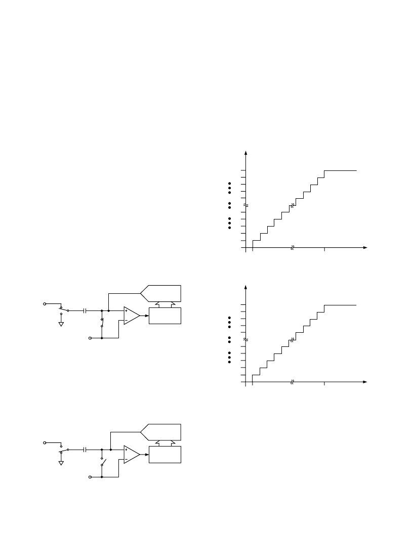
ADC TRANSFER FUNCTION
The output coding of the AD7476/AD7477/AD7478 is straight
binary. For the AD7476/AD7477, designed code transitions
occur midway between successive integer LSB values (i.e.,
1/2 LSB, 3/2 LSB, and so on). The LSB size for the AD7476
is V
DD
/4096 and the LSB size for the AD7477 is V
DD
/1024. The
ideal transfer characteristic for the AD7476/AD7477 is shown
in Figure 4.
For the AD7478, designed code transitions occur midway between
successive integer LSB values (i.e., 1 LSB, 2 LSB, and so on).
The LSB size for the AD7478 is V
DD
/256. The ideal transfer
characteristic for the AD7478 is shown in Figure 5.
1LSB = V
DD
/4096 (AD7476)
1LSB = V
DD
/1024 (AD7477)
ANALOG INPUT
111 ... 111
0V
0.5LSB
A
V
DD
–1.5LSB
111 ... 110
111 ... 000
011 ... 111
000 ... 010
000 ... 001
000 ... 000
Figure 4. Transfer Characteristic for the AD7476/AD7477
ANALOG INPUT
111 ... 111
0V
1LSB
A
V
DD
–1LSB
111 ... 110
111 ... 000
011 ... 111
000 ... 010
000 ... 001
000 ... 000
1LSB = V
DD
/256 (AD7478)
Figure 5. Transfer Characteristic for AD7478
TYPICAL CONNECTION DIAGRAM
Figure 6 shows a typical connection diagram for the AD7476/
AD7477/AD7478. V
REF
is taken internally from V
DD
and as
such, V
DD
should be well decoupled. This provides an analog
input range of 0 V to V
DD
. The conversion result is output in a
16-bit word with four leading zeros followed by the MSB of the
12-bit, 10-bit, or 8-bit result. The 10-bit result from the AD7477
will be followed by two trailing zeros. The 8-bit result from
the AD7478 will be followed by four trailing zeros.
相关PDF资料 |
PDF描述 |
|---|---|
| AD7476BRT-REEL | +3.3V, 2.125Gbps/1.0625Gbps Fibre-Channel Port Bypass ICs |
| AD7476BRT-REEL7 | 1 MSPS, 12-/10-/8-Bit ADCs in 6-Lead SOT-23 |
| AD7477AARM | Low-Power, 622Mbps Limiting Amplifiers with Chatter-Free Power Detect for LANs |
| AD7477AARM-REEL | 2.35 V to 5.25 V, 1 MSPS, 12-/10-/8-Bit ADCs in 6-Lead SC70 |
| AD7477AARM-REEL7 | +3.0V to +5.5V, 1.25Gbps/2.5Gbps Limiting Amplifiers |
相关代理商/技术参数 |
参数描述 |
|---|---|
| AD7476BRT-REEL | 制造商:AD 制造商全称:Analog Devices 功能描述:1 MSPS, 12-/10-/8-Bit ADCs in 6-Lead SOT-23 |
| AD7476BRT-REEL7 | 制造商:Analog Devices 功能描述:ADC Single SAR 600ksps 12-bit Serial 6-Pin SOT-23 T/R |
| AD7476BRTZ-R2 | 功能描述:IC ADC 12BIT 1MSPS SOT23-6 RoHS:是 类别:集成电路 (IC) >> 数据采集 - 模数转换器 系列:- 其它有关文件:TSA1204 View All Specifications 标准包装:1 系列:- 位数:12 采样率(每秒):20M 数据接口:并联 转换器数目:2 功率耗散(最大):155mW 电压电源:模拟和数字 工作温度:-40°C ~ 85°C 安装类型:表面贴装 封装/外壳:48-TQFP 供应商设备封装:48-TQFP(7x7) 包装:Digi-Reel® 输入数目和类型:4 个单端,单极;2 个差分,单极 产品目录页面:1156 (CN2011-ZH PDF) 其它名称:497-5435-6 |
| AD7476BRTZ-R23 | 制造商:AD 制造商全称:Analog Devices 功能描述:1 MSPS, 12-/10-/8-Bit ADCs in 6-Lead SOT-23 |
| AD7476BRTZ-REEL | 功能描述:IC ADC 12BIT 1MSPS SOT23-6 T/R RoHS:是 类别:集成电路 (IC) >> 数据采集 - 模数转换器 系列:- 标准包装:1,000 系列:- 位数:16 采样率(每秒):45k 数据接口:串行 转换器数目:2 功率耗散(最大):315mW 电压电源:模拟和数字 工作温度:0°C ~ 70°C 安装类型:表面贴装 封装/外壳:28-SOIC(0.295",7.50mm 宽) 供应商设备封装:28-SOIC W 包装:带卷 (TR) 输入数目和类型:2 个单端,单极 |
发布紧急采购,3分钟左右您将得到回复。