参数资料
| 型号: | AD7484BSTZ |
| 厂商: | Analog Devices Inc |
| 文件页数: | 9/20页 |
| 文件大小: | 0K |
| 描述: | IC ADC 14BIT SAR 3MSPS 48-LQFP |
| 标准包装: | 1 |
| 位数: | 14 |
| 采样率(每秒): | 3M |
| 数据接口: | 并联 |
| 转换器数目: | 1 |
| 功率耗散(最大): | 90mW |
| 电压电源: | 模拟和数字 |
| 工作温度: | -40°C ~ 85°C |
| 安装类型: | 表面贴装 |
| 封装/外壳: | 48-LQFP |
| 供应商设备封装: | 48-LQFP(7x7) |
| 包装: | 托盘 |
| 输入数目和类型: | 1 个单端,单极 |
| 产品目录页面: | 778 (CN2011-ZH PDF) |
| 配用: | EVAL-AD7484CBZ-ND - BOARD EVALUATION FOR AD7484 |
AD7484
Rev. C | Page 17 of 20
BOARD LAYOUT AND GROUNDING
For optimum performance from the AD7484, it is recommended
that a PCB with a minimum of three layers be used. One of
these layers, preferably the middle layer, should be as complete a
ground plane as possible to give the best shielding. The board
should be designed in such a way that the analog and digital
circuitry is separated and confined to certain areas of the board.
This practice, along with not running digital and analog lines close
together, helps to avoid coupling digital noise onto analog lines.
The power supply lines to the AD7484 are to be approximately
3 mm wide to provide low impedance paths and reduce the effects
of glitches on the power supply lines. It is vital that good decoupling
also be present. A combination of ferrites and decoupling capa-
citors should be used, as shown in Figure 23.The decoupling
capacitors are to be as close to the supply pins as possible. This
is made easier by the use of multilayer boards. The signal traces
from the AD7484 pins can be run on the top layer, while the
decoupling capacitors and ferrites can be mounted on the bottom
layer where the power traces exist. The ground plane between
the top and bottom planes provides excellent shielding.
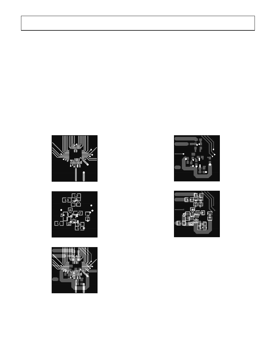
Figure 24 to Figure 28 show a sample layout of the board area
immediately surrounding the AD7484. Pin 1 is the bottom left
corner of the device. The black area in each figure indicates the
ground plane present on the middle layer. Figure 24 shows the
top layer where the AD7484 is mounted with vias to the bottom
routing layer highlighted. Figure 25 shows the bottom layer
silkscreen where the decoupling components are soldered
directly beneath the device. Figure 26 shows the top and bottom
routing layers overlaid. Figure 27 shows the bottom layer where
the power routing is with the same vias highlighted. Figure 28
shows the silkscreen overlaid on the solder pads for the
decoupling components, which are C1 to C6: 100 nF, C7 to C8:
470 nF, C9: 1 nF, and L1 to L4: Meggit-Sigma Chip Ferrite
Beads (BMB2A0600RS2).
02
64
2-
0
24
Figure 24. Top Layer Routing
02
64
2-
0
26
Figure 25. Bottom Layer Silkscreen
02
64
2-
0
28
Figure 26. Top and Bottom Routing Layers
02
64
2-
02
5
Figure 27. Bottom Layer Routing
0
26
42
-02
7
Figure 28. Silkscreen and Bottom Layer Routing
相关PDF资料 |
PDF描述 |
|---|---|
| AD7485BSTZ | IC ADC 14BIT SAR 1MSPS 48-LQFP |
| AD7490BRU-REEL | IC ADC 12BIT 16CH 28-TSSOP T/R |
| AD7492ARZ-5 | IC ADC 12BIT REF/CLOCK 24SOIC |
| AD7495BRM | IC ADC 12BIT SRL LP W/REF 8MSOP |
| AD75004KP | IC DAC 12BIT QUAD W/BUFF 28-PLCC |
相关代理商/技术参数 |
参数描述 |
|---|---|
| AD7484BSTZ | 制造商:Analog Devices 功能描述:IC 14-BIT ADC |
| AD7485 | 制造商:AMICC 制造商全称:AMIC Technology 功能描述:1 MSPS, Serial 14-Bit SAR ADC |
| AD7485BST | 制造商:Analog Devices 功能描述:ADC Single SAR 1Msps 14-bit Serial 48-Pin LQFP 制造商:Rochester Electronics LLC 功能描述:14 BIT, 1MSPS, SERIAL ADC I.C. - Tape and Reel 制造商:Analog Devices 功能描述:14BIT SERIAL ADC SMD 7485 LQFP48 |
| AD7485BSTZ | 功能描述:IC ADC 14BIT SAR 1MSPS 48-LQFP RoHS:是 类别:集成电路 (IC) >> 数据采集 - 模数转换器 系列:- 标准包装:1,000 系列:- 位数:12 采样率(每秒):300k 数据接口:并联 转换器数目:1 功率耗散(最大):75mW 电压电源:单电源 工作温度:0°C ~ 70°C 安装类型:表面贴装 封装/外壳:24-SOIC(0.295",7.50mm 宽) 供应商设备封装:24-SOIC 包装:带卷 (TR) 输入数目和类型:1 个单端,单极;1 个单端,双极 |
| AD7490 | 制造商:AD 制造商全称:Analog Devices 功能描述:16-Channel, 1 MSPS, 12-Bit ADC with Sequencer in 28-Lead TSSOP |
发布紧急采购,3分钟左右您将得到回复。